As microchips shrink, even tiny defects in the lines, dots and other shapes etched on them become major barriers to performance. Princeton engineers have now found a way to literally melt away such defects, using a process that could dramatically improve chip quality without increasing fabrication cost.
The method, published in the May 4 issue of Nature Nanotechnology, enables more precise shaping of microchip components than what is possible with current technology. More precise component shapes could help manufacturers build smaller and better microchips, the key to more powerful computers and other devices.
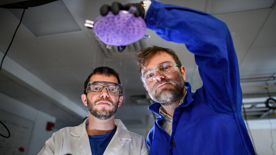
"We are able to achieve a precision and improvement far beyond what was previously thought achievable," said electrical engineer Stephen Chou, the Joseph C. Elgin Professor of Engineering, who developed the method along with graduate student Qiangfei Xia. Chou's lab has previously pioneered a number of innovative chip making techniques, including a revolutionary method for making nanometer-scale patterns using imprinting.
Microchips work best when the structures fabricated on them are straight, thin and tall. Rough edges and other defects can degrade or even ruin chip performance in most applications. In integrated circuits, for instance, such flaws could cause current to leak and voltage to fluctuate. In optic devices, they could interfere with the transmission of light. In biological devices, they could impede the flow of DNA and other biomaterials.
"These chip defects pose serious roadblocks to future advances in many industries," Chou said.
To deal with this problem, researchers try to improve the process used to make the microchips. However, Chou said such an approach works only to a point; eventually chip makers will run up against fundamental physical limits of current manufacturing techniques. In particular, the electrons and photons that are used like chisels to carve out the microscopic features on a chip always have some random behavior. This effect becomes pronounced at very small scales and limits the accuracy of component shapes.
"What we propose instead is a paradigm shift: Rather than struggle to improve fabrication methods, we could simply fix the defects after fabrication," said Chou. "And fixing the defects could be automatic -- a process of self-perfection."
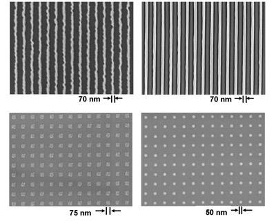
These electron microscope images show before (left column) and after (right column) examples of a new technique, developed at Princeton University, for perfecting nanometer-scale structures. (Stephen Chou/Nature Nanotechnology)
Chou's method, termed Self-Perfection by Liquefaction, achieves this by melting the structures on a chip momentarily, and guiding the resulting flow of liquid so that it re-solidifies into the desired shapes. This is possible because natural forces acting on the molten structures, such as surface tension -- the force that allows some insects to walk on water -- smooth the structures into geometrically more accurate shapes. Lines, for instance, become straighter, and dots become rounder.
Simple melting by direct heating has previously been shown to smooth out the defects in plastic structures. This process can't be applied to a microchip for two reasons. First, the key structures on a chip are not made of plastic, which melts at temperatures close to the boiling point of water, but from semiconductors and metals, which have much higher melting points. Heating the chip to such temperatures would melt not just the structures, but nearly everything else on the chip. Second, the melting process would widen the structures and round off their top and side surfaces, all of which would be detrimental to the chip.
Chou's team overcame the first obstacle by using a light pulse from a so-called excimer laser, similar to those used in laser eye surgery, because it heats only a very thin surface layer of a material and causes no damage to the structures underneath. The researchers carefully designed the pulse so that it would melt only semiconductor and metal structures, and not damage other parts of the chip. The structures need to be melted for only a fraction of a millionth of a second, because molten metal and semiconductors can flow as easily as water and have high surface tension, which allows them to change shapes very quickly.
To overcome the second obstacle, Chou's team placed a thin quartz plate on top of the melting structures to guide the flow of liquid. The plate prevents a molten structure from widening, and keeps its top flat and sides vertical, Chou said. In one experiment, it made the edges of 70 nanometer-wide chromium lines more than five times smoother. The resulting line smoothness was far more precise than what semiconductor researchers believe to be attainable with existing technology.
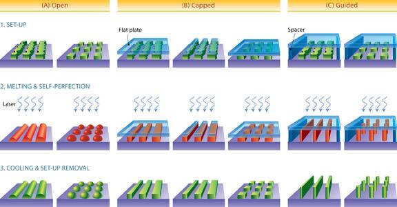
A technique invented in the lab of Princeton engineer Stephen Chou allows for the easy correction of defects and refinement of shapes in nanostructures. The "open" method involves using a laser to briefly melt defects, which self-correct before cooling. The "capped" method prevents the technique from rounding off the structures. The "guided" version causes the structures to grow toward a nearby plate, causing them to become not only smoother, but taller and thinner, which are all desirable traits for creating smaller, more powerful computer chips. (Stephen Chou/Nature Nanotechnology)
The conventional approach to fixing chip defects is to measure the exact shape of each defect, and provide a correction precisely tailored to it -- a slow and expensive process, Chou said. In contrast, Chou's guided melting process fixes all defects on a chip in a single quick and inexpensive step. "Regardless of the shape of each defect, it always gets fixed precisely and with no need for individual shape measurement or tailored correction," Chou said.
One of the big surprises from this work is observed when the guiding plate is placed not in direct contact with the molten structures, but at a distance above it. In this situation, the liquid material from the structures rises up and reaches the plate by itself, causing line structures to become taller and narrower -- both highly desirable outcomes from a chip design perspective.
"The authors demonstrate improved edge roughness and dramatically altered aspect ratios in nanoscale features," said Donald Tennant, director of operations at the NanoScale Science and Technology Facility at Cornell University. The techniques "may be a way forward when nanofabricators bump up against the limits of lithography and pattern transfer," he said.
Next, Chou's group plans to demonstrate this technique on large (8-inch) wafers. Several leading semiconductor manufacturers have expressed keen interest in the technique, Chou said.
The work was supported by the Defense Advanced Research Projects Agency and the Office of Naval Research.