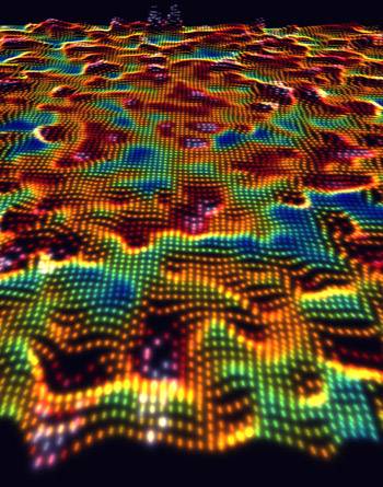
On the brink of the metal-insulator transition, the electrons in a manganese-doped gallium arsenide semiconductor are distributed across the surface of the material in complex, fractal-like patterns. These shapes are visible in this electron map, where the colors red, orange and yellow indicate areas on the surface of the semiconductor where electrons are most likely to be found at a given point in time. In this image, the fractal-like probability map of electrons is superimposed on the atomic crystal structure of the material, imaged at the same time. (Image: Roushan/Yazdani Research Group)(Image for news media)
* Read about another Princeton University-led team making advances in spintronics *
Just as the heartbeats of today's electronic devices depend on the ability to switch the flow of electricity in semiconductors on and off with lightning speed, the viability of the "spintronic" devices of the future -- technologies that manipulate both the flow and magnetic "spin" of electrons -- will require similarly precise control over semiconductor magnetism.
Achievement of this goal necessitates a detailed understanding of what happens at the exact transition point when a semiconductor changes from a metal to an insulator -- a phenomenon shrouded in mystery despite decades of examination.
But in results published Feb. 5 in the journal Science, a Princeton-led team of scientists has observed electrons in a semiconductor on the brink of the metal-insulator transition for the first time. Caught in the act, the electrons formed complex patterns resembling those seen in turbulent fluids, confirming some long-held predictions and providing new insights into how semiconductors can be turned into magnets. The work also could lead to the production of smaller and more energy-efficient computers.
"The spatial structure of the electron waves inside a given material determines how well it conducts electricity," said team leader Ali Yazdani, a Princeton professor of physics. "If the waves extend throughout the material, we get metallic behavior, but if they get localized, or stuck, in specific regions, electricity stops flowing. The way in which electrons undergo this transition in certain semiconductors also appears to play a big role in how they become magnetic."
In their natural state, semiconductors such as silicon or gallium arsenide are insulators that do not conduct electricity. For decades, scientists have known that they can transform these insulators into metals, which conduct electricity, by replacing some of the atoms in the chemical lattice structure with other atoms, for instance, replacing the gallium in gallium arsenide with zinc or manganese. This process, called doping, changes the number of electrons in the material to enable the flow of electricity, but also introduces disorder into the lattice structure that can hinder the electrons' movement and cause them to become "stuck," or localized. Conduction is able to occur only if the electrons can "hop" from atom to atom in the structure, slaloming among the randomness and disorder where the lattice has been perturbed.
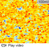
This video depicts electron wave functions, measured in a manganese-doped gallium arsenide semiconductor, based on their energy, illustrating an example of extended and localized electron states and the transition between them. The colors red, orange and yellow indicate areas on the surface of the semiconductor where electrons are most likely to be found at a given point in time, while blue and green indicate areas where electrons are unlikely to be found. At the beginning of the video, the electrons are extended across the surface of the semiconductor, as in a metal. At the brink of transition, which occurs when the energy level in the upper right hand corner is zero mV, the electrons are distributed in intricately shaped "fractal puddles." After crossing this divide, the semiconductor becomes increasingly insulator-like and the electrons are clumped together in small regions, having been trapped, or localized, by the disorder in the material. (Video: Yazdani Lab)
The idea of electron localization goes back to the seminal work of Princeton's Joseph Henry Professor of Physics Emeritus Philip Anderson, who won the Nobel Prize in 1979 in part for proposing that localization can occur for "quantum" particles, including electrons, when they encounter random obstacles, such as in doped semiconductors. While research over the decades has found evidence for Anderson localization in many materials, the electron waves undergoing this transition never before have been visualized directly. At the transition point, computer simulations have long predicted the emergence of complex non-uniform patterns of electron waves, like the flow of water in a rocky river.
Yazdani's team originally set out to understand how doping a gallium arsenide semiconductor with manganese atoms could convert it into a magnet and "turn on" electrical conductivity in the compound. After team members at the University of California-Santa Barbara added manganese atoms to the lattice structure, the researchers used specially designed scanning tunneling microscopes at Princeton to visualize the electron states in the material.
Finding themselves confronted with complex spatial patterns of electron waves, the scientists realized that the patterns they saw were in fact those predicted for electrons on the brink of localization. In these patterns, the majority of the electrons are distributed across the surface of the semiconductor in a series of interconnected "puddles" that resemble fractals -- self-similar shapes that repeat themselves on increasingly smaller-length scales. Fractals commonly are associated with objects in nature, such as coastlines or snowflakes, but they have never before been seen for quantum particles.
These observed patterns have important implications for how a semiconductor becomes a magnet. All electrons have a property called "spin," which describes the way they rotate on their axes, generating a magnetic field as they do so. If the spins of neighboring electrons in a given material are opposite one another, these magnetic fields cancel each other out. But when the spins of neighboring electrons in a material are aligned, such that the electrons are rotating in tandem like synchronized swimmers in a pool, the material itself becomes magnetic. This alignment only occurs among the electrons of certain elements, including iron and manganese.
While it was assumed that magnetism in manganese-doped gallium arsenide occurs because the spins of all the manganese electrons in the doped semiconductor become aligned uniformly, the team's results suggested this is not the case: The alignment of spins depended on the location of electrons within the fractal puddles, indicating that there are likely areas of strong and weak magnetic interaction in the material.
"We have shown that electrons move and live in these jagged puddles, so it is only natural to consider that manganese atoms that reside within each puddle are interacting with each other and giving rise to the magnetism," Yazdani said. "In this view, where the puddles are not, we have manganese atoms but they are not interacting or contributing to magnetism. The puddles become part of the story to understand how magnetism comes about."
Manganese-doped gallium arsenide has been at the heart of many recent technological advances, and a precise understanding of what causes magnetism in these semiconductors -- and how to control it -- will be necessary for the realization of one of the most promising applications of the material: computer chips able to both process and store information. In current devices, chips made of semiconductors, such as silicon, are used to process information, which is then stored in hard drives made out of magnetic materials, such as iron. If the magnetism of a material could be switched on and off, the same chip could be used for both purposes, paving the way for smaller and more energy-efficient computers.
In the future, the team intends to explore the connection between optimizing magnetism and the shape of the fractal puddles to find further clues for the mechanism of magnetism and develop ways to enhance it. Their techniques also will allow them to explore whether electrons form similar patterns at the brink of other phase transitions, such as from conductivity to superconductivity.
Yazdani's Princeton colleagues on the team were physics professor David Huse and graduate students Anthony Richardella, also of the University of Illinois-Urbana/Champaign, Pedram Roushan and Brian Zhou. The research team also included Shawn Mack and David Awschalom of the University of California-Santa Barbara. The work was funded by the National Science Foundation, the Office of Naval Research and the Army Research Office.