Above the Fray
Keith Morton GS
Department of Electrical Engineering
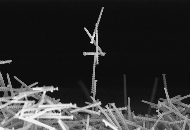
Scanning electron micrograph of 300nm diameter high-aspect ratio silicon pillars made using nanoimprint lithography and deep reactive ion etching. The original, regular array of pillars was part of a microfluidic device to separate nanoparticles. The pillars pile up from scribing damage when the silicon wafer is cleaved to obtain a cross-section image.
|