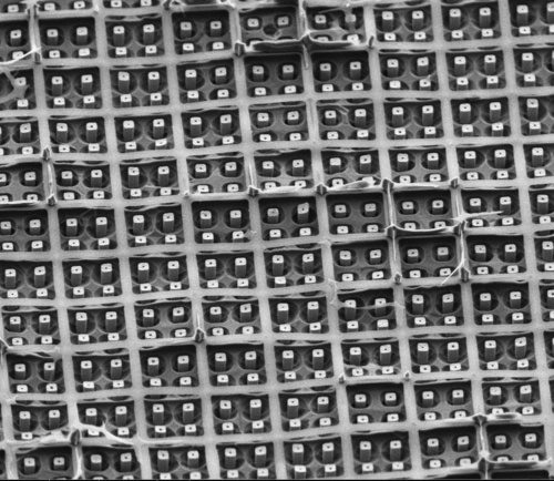
A via is a vertical electrical connection between different layers of conductors in a physical electronic circuit. These 1.24um by 1.24um vias were exposed after etching off one of the metal layers fabricated by IBM CMOS processing. Silicon dioxide around the vias got etched away -- digging a hole around them. The thin silicon nitride layer on oxide stayed intact during the oxide etch, making it look as if the thin layer is floating.
REVISED