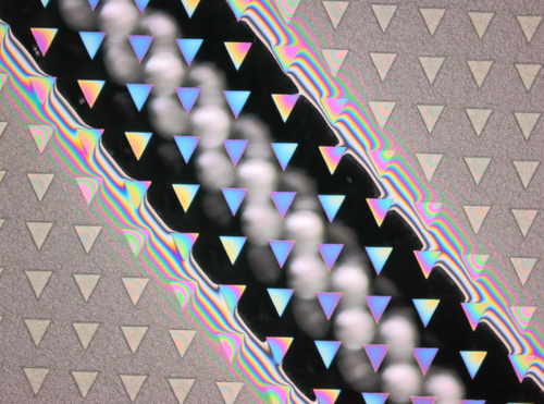
This photograph shows a silicon device after a reactive ion etch. The device is patterned with an oxide layer (light brown) to define device structures and a photoresist layer (dark brown) to protect the structures during a through wafer etch. An errant speck of dust caused a streak in the photoresist that thinned this protective layer in one region. During the etch, the thinned photoresist was torn away, leaving a chasm spanned by triangular pillars.