WHY?
Organic semiconductors have been the subject of intense research in the past decades because of their applications in electronic and optoelectronic devices [1]. Although organic electronics are still far from (and actually not expected to be) replacing the high-end semiconductor devices, they are very promising in applications where elasticity, reduced cost, and ease of production are needed which cannot be provided by the current silicon based devices. Organic electronic devices generally employ thin films of the semiconductor material as the active region (where charge is carried). Thus one needs to improve the film quality to get better device characteristics.
HOW?
To achieve the goal of producing best quality films (e.g. large grain size, small number of charge traps) several techniques have been employed such as spinning, vapor phase deposition and Langmuir Blodgett deposition [2, 3]. The best results were obtained by vapor phase deposition and several derivatives of this technique have been developed in order to control the growth parameters more precisely [1, 4, 5]. Base pressure of the deposition system, substrate temperature, deposition rate and the purity of the organic source material are the most important parameters, which determine the impurity concentration in the film and the adsorption dynamics of molecules on the substrate (e.g. diffusion length). Recently, Iannotta and co-workers have developed a supersonic molecular beam (SSB) source that allows to control of the film growth by varying the velocity of the deposited molecules [6, 7]. The source is of the "seeded beam" in which the vapor of an organic molecule is seeded into a flow of carrier gas expanding this mixture supersonically thorough a nozzle. By changing the seeding ratio, they were able to change the kinetic energy of the molecules which in turn determines (among the other parameters) the diffusion length on the surface. Our aim is to use He atom diffraction as a probe to characterize pentacene thin films grown on metal and insulator substrates by using the SSB source developed by Ianotta and co-workers, and to find out quantitatively whether this new source improves film properties or not.
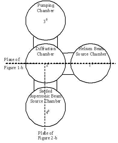
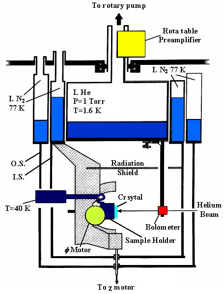
Our experimental apparatus consists of four chambers which
house the supersonic helium beam source (Chamber 1) (probe beam used for
He atom diffraction), the bolometer detector/crystal manipulator assembly
(Chamber 2), a refrigerated trap to ensure an oil-free high vacuum (Chamber
3), and the seeded supersonic beam source (Chamber 4) (secondary beam used
for producing the films). Chambers 1 and 2 and 2 and 4 are separated by
diaphragms with a collimator placed on their respective beam axis. Chambers
2 and 3 are instead basically a single chamber. A cold supersonic helium
beam is produced in chamber # 1 by expansion through a 20 µm nozzle.
This beam strikes the sample in the chamber # 2 and the diffracted atoms
are detected by a bolometer that is rotatable around the sample in the
plane containing surface normal and the incident He beam. Azimuthal, polar,
and tilt rotation of the sample holder enables us to map a good fraction
of the reciprocal space. The SSB source is located in chamber no 3. Organic
molecules are seeded in a flux of either helium or krypton atoms and the
mixture expands supersonically through a 100 µm nozzle and hits the
sample. As the organic molecules sticks to the sample surface the specular
intensity decays. From this initial decay, information about the flux of
the organic molecules on the surface and the adsorption mechanism can be
obtained. The surface unit cell structure of the film can be determined
from the diffraction pattern of He atoms.
|
|
|
Figure 1 a) Schematic of the diffraction apparatus. b) A detailed sketch of the inner part of diffraction chamber
WHAT HAVE WE DONE SO FAR?
We have finished the optimization of the SSB source a few months ago and recently completed a detailed study of growth of pentacene thin films on Ag(111). During this study the effect of kinetic energy on the film growth have been investigated by changing the carrier gas from Helium to Krypton which reduces the energy by a factor of ~10. The effect of substrate temperature on film growth has also been investigated. We also have performed X-ray diffraction measurements in order to determine the periodicity and the thickness of the pentacene film.
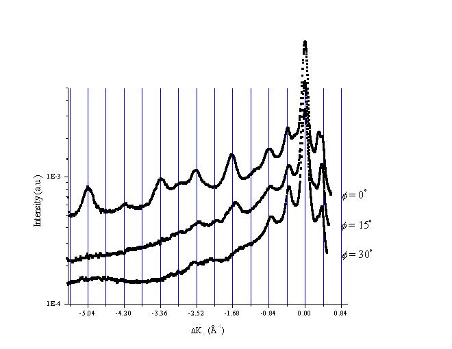
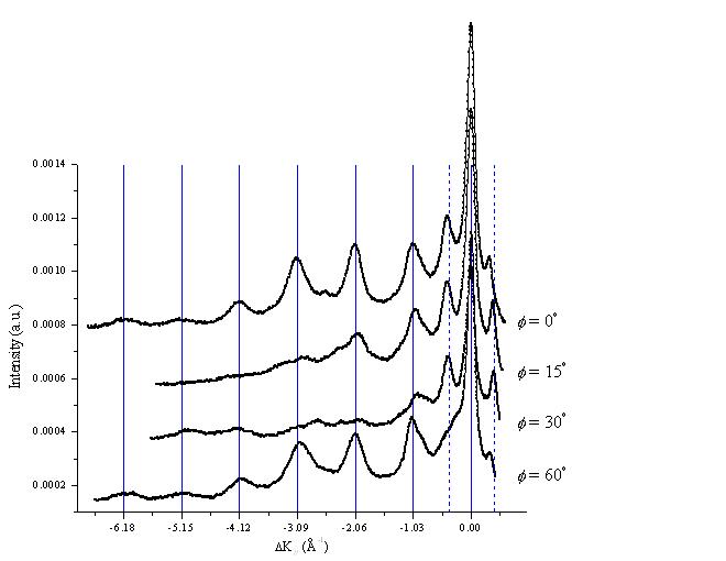
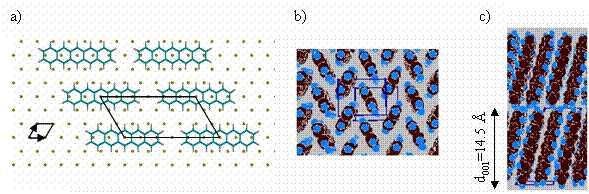
We found that a pentacene monolayer grown by using He carrier gas forms a (6x3) super lattice of Ag(111) (figure 2a, figure 3a). This is a close packed structure commensurate to the underlying substrate with unit cell dimensions 17.28 Å x 8.64 Å. When deposition is continued further a multilayer, which has a different structure than the monolayer is obtained (figure 2b). The diffraction pattern fits well with a rectangular unit cell of dimensions 6.22 Å x 15.6 Å. These dimensions suggest that pentacene molecules adopt a unit cell that is very close to the bulk lattice. We think molecules form layers with a similar arrangement to that of b-c plane of the single crystal (figure 2b,c). The thickness of each layer, 3.7 Å, found by synchrotron X-ray diffraction, which is about the half of a-unit cell dimension (3.95 Å) of the bulk lattice also supports this model. We also studied the effect of substrate temperature on the film growth. The optimum temperature for the film growth is found to be 200K. Although the monolayer structure was similar, for all the substrate temperatures (150K, 200K, 250K) the multilayer peaks were quite broad for the films grown at 150K and 250K. Annealing of these films to 300K improved the diffraction pattern and resulted in a partial decrease in the peak widths, which is an indication of increased domain size. Here it should be noted that diffusion length of the molecules on the substrate may not be the only parameter responsible for the island size, since multilayer quality grown at 250 K is not as good as that of 200 K grown films although the temperature (and in turn the diffusion length) is higher.
When, the kinetic energy of the pentacene molecules is
decreased by using Kr carrier gas, we observed a monolayer structure that
is the same as that of a monolayer grown using He as carrier gas. However
multilayer diffraction peaks were considerably broad. Upon annealing peaks
get narrower which is an indication of increasing domain size. It should
be noted that even after annealing diffraction pattern of films grown by
using Kr carrier gas was not as good as that of none annealed He grown
films. These results are quite promising since, to our knowledge, this
is the first time that structural difference between the first layer and
multilayers of an organic semiconductor on a metal substrate and the effect
of kinetic energy on film growth has been directly demonstrated using diffractive
probe.
 |
 |
To clarify he submonolayer structure in more detail, we plan to perform a back-reflection X-ray standing waves experiment. From the analysis of the results we hope to reconstruct the atomic height positions of the carbon atoms respective to the Ag surface before and at complete monolayer coverage. This will indicate whether the molecules are initially lying flat on the Ag surface, and if they remain in that position also when the film consists of several layers. Furthermore, we hope to explore the nature of possible structural changes during or after the monolayer completion.
In addition to silver substrates we plan to investigate
pentacene thin films on insulator and chemically treated metal substrates,
since the latter are more interesting from an applied point of view. Especially
for transistor fabrication one needs to form organic thin films on an insulator
substrate which acts as the gate dielectric. The common choice for such
kind of substrates is SiO2. The adsorption of organic molecules
on hydrogen terminated or bare silicon are also in interest. Therefore
our next goal is to study the adsorption of pentacene on SiO2
and hydrogen terminated silicon. However preparing smooth silicon surfaces,
either hydrogen or oxygen terminated, is quite tricky and in our first
attempts we could not obtain a smooth enough surface for He diffraction.
At the moment we are trying to produce smooth hydrogen terminated silicon
surfaces to be used in He diffraction measurements by using several different
wet chemistry procedures. We also plan to use AFM to study the morphology
of films prepared with the SSB source and check their electrical transport
properties.
References
[1] S. R. Forrest, Chem. Rev. 97, 1793, (1997) and references therein
[2] Horowitz G. "Organic field-effect transistors" Adv. Mater. 10, 365 (1998) and references therein.
[3] Dimitrakopoulos C.D., Malenfant P.R.L., "Organic thin film transistors for large area electronics" Adv. Mater. 14, 99 (2002) and references therein.
[4] Kloc Ch., Simpkins P.G., Siegrist T., Laudise R.A., "Physical vapor growth of centimeter-sized crystals of a -hexasexithiophene" J. Cryst. Growth 182, 416 (1997)
[5] Baldo M., Deutsch M., Burrows P., Gossenberger M., Gerstenberg V. Ban, Forrest S., "" Adv. Mater. 10, 1505 (1998).
[6] Iannotta S., Toccoli T., Biasioli F., Boschetti A., Ferrari M., "Highly ordered films of quaterthiophene grown by seede supersonic beams" Appl. Phys. Lett. 76, 1845 (2000).
[7] Iannotta S., Toccoli T., Boschetti A., Scardi P.,
"Optical properties, morphology and structure of high quality oligothiophene
films grown by supersonic seeded beams" Synth. Met. 122, 221 (2001).