
![]()
HOME | TEXT | GRADING | STAFF | PROGRESS | LECTURES | LABS | CIRCUITS |PROGRAMS
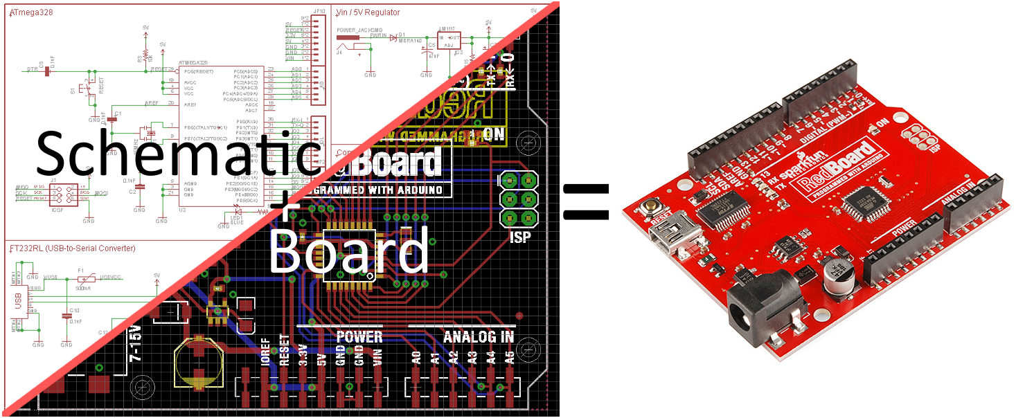
Printed circuit boards (PCBs) are the backbone of every electronic gizmo out there. They're not flashy like those microprocessors, or abundant like resistors, but they're essential to making all components in a circuit connect together just right.
We LOVE designing PCBs here at SparkFun. It's a love that we want to spread. It's a skill that benefits electronics enthusiasts of every caliber. Through this and a series of tutorials, we'll explain how to design a PCB using EAGLE: the same software we use to design all of our PCBs.
This first tutorial goes over how to install the software, and tailor-fit its interface and support files.
EAGLE is one of many PCB CAD softwares out there. So you might ask: âWhat makes EAGLE so special?â We're fond of EAGLE for a few reasons in particular:
Of course, EAGLE has its drawbacks too. More powerful PCB design tools out there might have a better autorouter, or nifty tools like simulators, programmers, and 3D viewers. For us though, EAGLE has everything we need to design simple-to-intermediate PCBs. It's an excellent place to start if you've never designed a PCB before.
EAGLE is available on Cadsoft's (the developer company) download page. Grab the most recent version that matches your operating system (the software is available for Windows, Mac and Linux). It's a relatively light download: about 45MB.
EAGLE installs just like any old program, it'll self extract and then present you with a series of dialogs to configure the installation.
On the last screen of the installation process, you should be presented with a window like this:
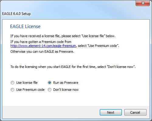
One of our favorite things about EAGLE is that it can be used for free! There are a few limitations to be aware of when using the free version:
Those limitations still make EAGLE an amazing piece of software. Engineers here at SparkFun could design 99% of our boards using the freeware version, if not for that pesky non-profit stipulation. You still have access to all phases of the EAGLE software, including the Autorouter.
If you need to upgrade your license there are a few versions available. Most licenses are still incredibly low priced (in comparing to the other stuff out there).
The first time you open up EAGLE, you should be presented with the Control Panel view. The Control Panel is the âhomebaseâ for Eagle, it links together all of the other modules in the software.
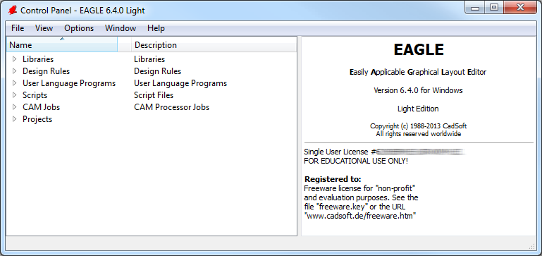
You can explore the six separate trees in the control panel, which highlight separate functions of the software:
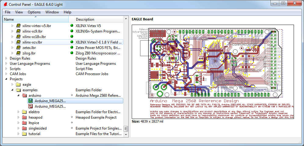
If you select a file in a tree, information about it will appear in the right-hand portion of the window. This is a great way to explore libraries, project designs (EAGLE comes with some fun examples), or to get a good overview of what a script's purpose is.
Included with EAGLE is an impressively list of part libraries, which you can explore in the Control Panel view. There are hundreds of libraries in here, some devoted to specific parts like resistors, or NPN transistors, others are devoted to specific manufacturers. This is an amazing resource! But it can also be a bit overwhelming. Even if you just want to add a simple through-hole electrolytic capacitor, there are dozens of libraries and parts to sort through to find the right thing.
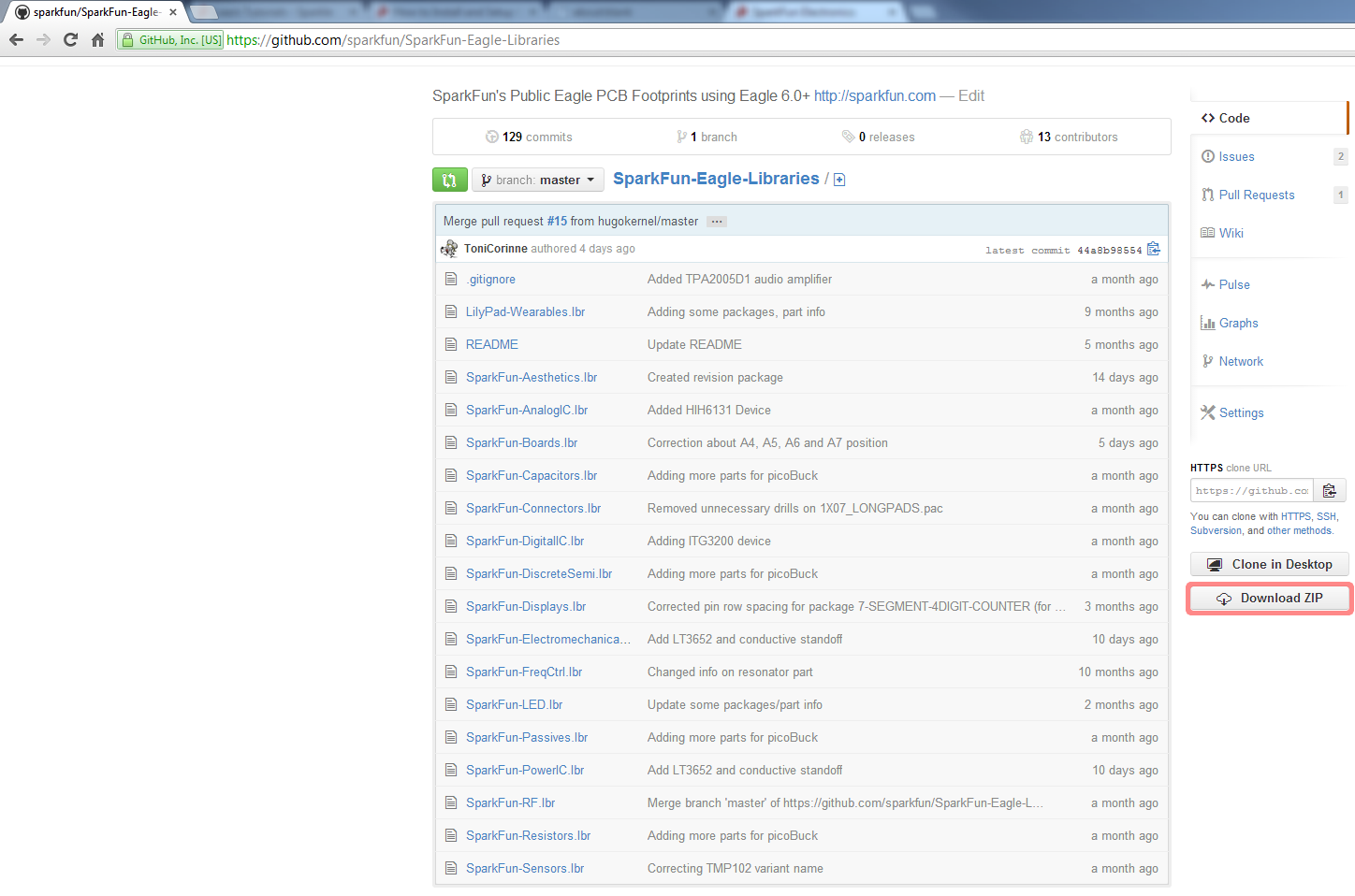
Instead of using the hundreds of default libraries, you can use the SparkFun EAGLE Libraries, which are filtered down to only include the parts that weâve used in designs ourselves. And theyâre constantly updated with new parts weâve discovered.
Hereâs how you can install and use the SparkFun libraries instead of (or in addition to) the default ones:
The most recent version of the libraries can always be found in the GitHub repository. Basically, all youâll need to do from the main repository page is click âDownload ZIPâ.
Save the ZIP file somewhere handy. Then extract the folder â donât forget where it is!
Back to the EAGLE Control Panel window now. Go to the âOptionsâ menu and then select âDirectoriesâ. This is a list of computer directories where EAGLE looks when it populates all six objects in the tree viewâ¦including libraries.
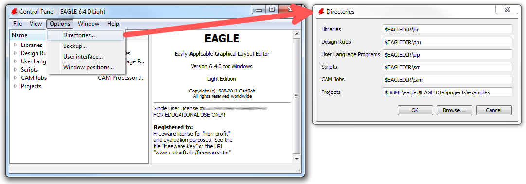
In the âLibrariesâ box is where weâll add a link to the directory where the SparkFun EAGLE libraries are stored. There are a few options here. If youâd like to keep the default libraries and add the SparkFun library, add a semicolon (;) after â$EAGLEDIR\lbrâ, and paste the SparkFun EAGLE Libraries directory location after that.
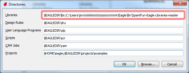
Note: Mac and Linux users should place a colon (:) between directories instead of the semicolon.
Now, when you go back and look at the âLibrariesâ tree, there should be two folders included, one of which should be our SparkFun Eagle Libraries. The last step is to tell EAGLE that, for now at least, we donât want to use the default libraries. To do this, right click on the âlbrâ folder, and select âUse noneâ.
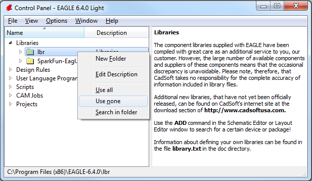
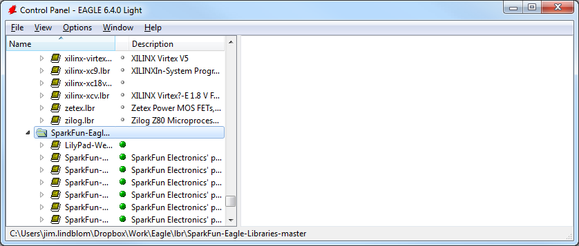
Then, right-click on the âSparkFun-Eagle-Libraries-masterâ folder, and select âUse allâ. Then check the libraries in each of the two folders. Next to them should be either a grey or green dot. A green dot next to a library means itâs in use, a grey dot means itâs not. Your libraries tree should look a little something like this:
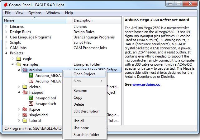
EAGLE is packaged with a handful of nifty example PCB designs. Open one up by expanding the âProjectsâ tree. From there, under the âexamplesâ folder open up the âarduinoâ project by double-clicking the red folder (or right-clicking and selecting âOpen projectâ). Note that, in this view, project folders are red and regular folders are the standard yellow.
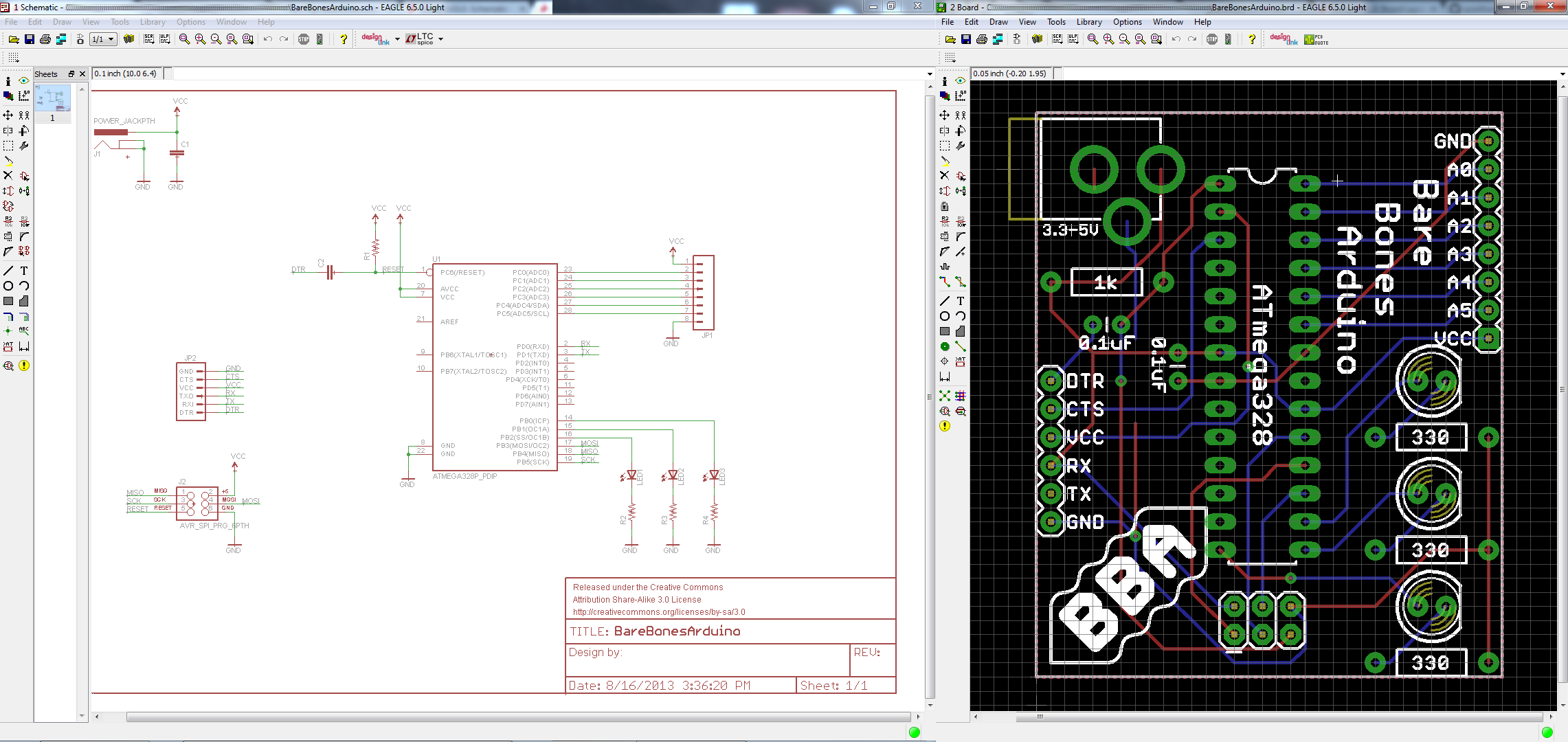
Opening the project should cause two more EAGLE windows to spawn: the board and schematic editors. These are the yin and the yang of EAGLE. They should be used together to create the finished product that is a functional PCB design.
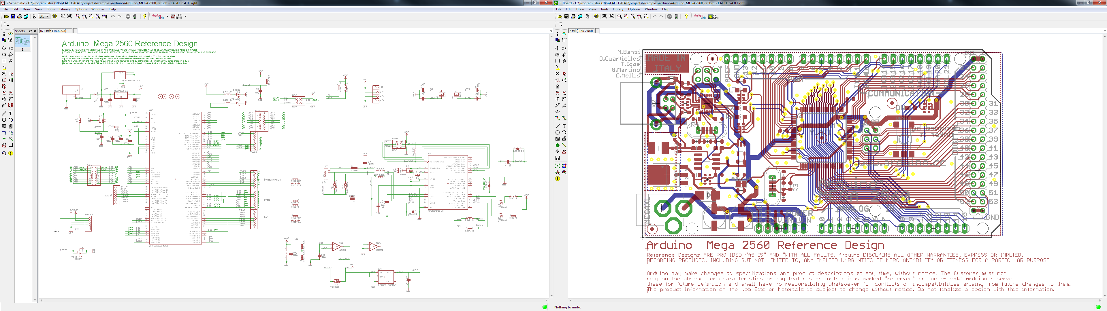
Schematic (left) and board editors both open. Click to embiggen.
The schematic editor (on the left above) is a collection of red circuit symbols which are interconnected with green nets (or wires). A project's schematic is like the comments in a program's code. It helps tell the story of what the board design actually does, but it doesn't have much influence on the end product. Parts in a schematic aren't precisely measured, they're laid out and connected in a way that's easy to read, to help you and others understand what's going on with the board design.
The board editor is where the real magic happens. Here colorful layers overlap and intersect to create a precisely measured PCB design. Two copper layers: red on top, blue on the bottom: are strategically routed to make sure different signals don't intersect and short out. Yellow circles (on this design, but they're more often green) called âviasâ pass a signal from one side to the other. Bigger vias allow for through-hole parts to be inserted and soldered to the board. Other, currently hidden, layers expose copper so components can be soldered to it.
Both of these windows work hand-in-hand. Any changes made to the schematic are automatically reflected in the board editor. Whenever you're modifying a design it's important to keep both windows open at all times.
If, for instance, you closed the board window of a design, but continued to modify a schematic. The changes you made to the schematic wouldn't be reflected in the board design. This is bad. The schematic and board design should always be consistent. It's really painful to backtrack any changes in an effort to reattain consistency. Always keep both windows open!
There are a few ways to tell if you don't have consistency between windows. First, there's a âdotâ in the lower-right hand corner of both windows. If the dot is green, everything is groovy. If the dot is magenta, a window's probably closed that shouldn't be. Second, and more obvious, if you close either of the two windows a big, huge warning should pop up in the other:
If you see that warning STOP doing anything, and get the other window back open. The easy way to get either a board or schematic window back open is by clicking the âSwitch to board/schematicâ icon:  /
/  (also found under the âFileâ menu).
This is a subject that's usually glazed over, but it's important to know how to navigate around both of these windows.
To move around within an editor window, a mouse with a scroll wheel comes in very handy. You can zoom in and out by rotating the wheel forward and backward. Pressing the wheel down, and moving the mouse allows you to drag the screen around.
If you're stuck without a three-button mouse, you'll have to resort to the view options to move around the editor views. All of these tools are located near the middle of the top toolbar, or under the âViewâ menu. The zoom in:  : and zoom out:
  : tools are obviously handy. So is the âZoom selectâ tool:
  : which alters the view to your selection. But really, if you're serious about using EAGLEâ¦get a mouse!
EAGLE's user interface is highly customizable. Anything from the background color, to layer colors, to key bindings can be modified to fit your preference. Better tailoring your interface can make designing a PCB much easier. On this page we'll talk about how we at SparkFun prefer to customize our UI. None of these steps are required. Customize your UI as you see fit. These are just the settings that we've grown accustomed to.
The first adjustment we always make to the UI is the background color of the board editor. The standard white background doesn't always meld very well with the array of colored layers required for board design. Instead, we usually opt for a black background.
To change the background color, go up to the âOptionsâ menu and select âUser interfaceâ.
Inside the âLayoutâ box you can set the background to black, white, or a specific color.
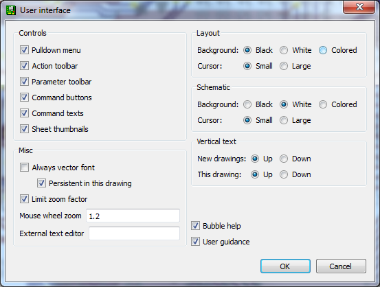
There are other options in this box to be explored, but you may want to hold off on adjusting most until you have more experience with the software.
Another UI improvement we like to make in the board editor is turning the grid on. Dimensions and sizes are so important to the design of your PCB, having some visible reminders of size can be very helpful. To turn the grid view on, click the  icon near the top-left corner of the board window (or go to the âViewâ menu and select âGridâ).
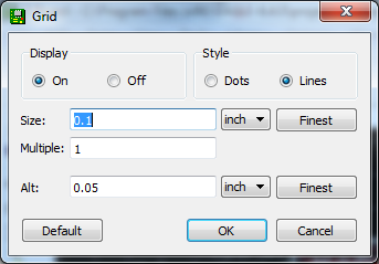
Switch the âDisplayâ radio button over to âOnâ. We'll also make the grid a bit less fine by setting the âSizeâ to 100 mil (0.1") and âAltâ to 50 mil (0.05").
PCB design in EAGLE is a two-step process. First you design your schematic, then you lay out a PCB based on that schematic. EAGLE's board and schematic editors work hand-in-hand. A well-designed schematic is critical to the overall PCB design process. It will help you catch errors before the board is fabricated, and it'll help you debug a board when something doesn't work.
This tutorial is the first of a two-part Using EAGLE series, and it's devoted entirely to the schematic-designing side of EAGLE. In part 2, Using EAGLE: Board Layout, we'll use the schematic designed in this tutorial as the basis for our example board layout.
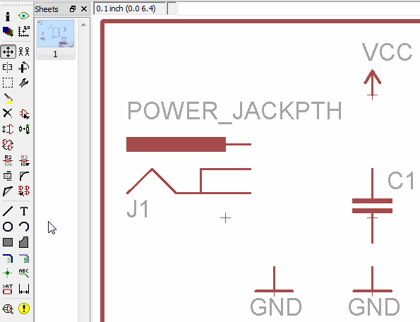
We'll start by making a new project folder for our design. In the control panel, under the âProjectsâ tree, right click on the directory where you want the project to live (by default EAGLE creates an âeagleâ directory in your home folder), and select âNew Projectâ.
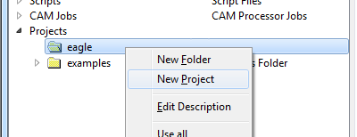
Give the newly created, red project folder a descriptive name. How about âBare Bones Arduinoâ.
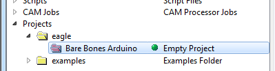
Project folders are like any regular file system folder, except they contain a file named âeagle.epfâ. The EPF file links your schematic and board design together, and also stores any settings you may have set especially for the project.
The project folder will house both our schematic and board design files (and eventually our gerber files too). To begin the design process, we need to lay out a schematic.
To add a schematic to a project folder, right-click the folder, hover over âNewâ and select âSchematicâ.
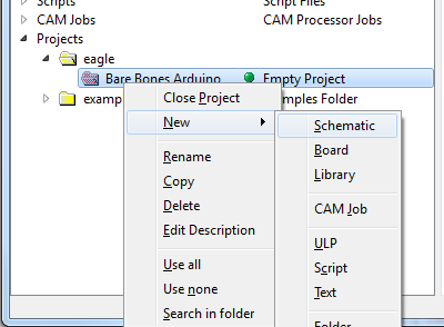
A new, blank window should immediately pop up. Welcome to the schematic editor!
Schematic design is a two step process. First you have to add all of the parts the schematic sheet, then those parts need to be wired together. You can intermix the steps: add a few parts, wire a few parts, then add some more: but since we already have a reference design we'll just add everything in one swoop.
The ADD tool:  (on the left toolbar, or under the Edit menu): is what you'll use to place every single component on the schematic. The ADD tool opens up a library navigator, where you can expand specific libraries and look at the parts it holds. With a part selected on the left side, the view on the right half should update to show both the schematic symbol of the part and its package.
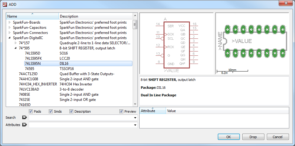
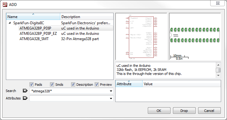
The ADD tool also has search functionality: very helpful when you have to navigate through dozens of libraries to find a part. The search is very literal, so don't misspell stuff! You can add wildcards to your search by placing an asterisk (*) before and/or after your search term. For example if you search for atmega328 you should find a single part/package combo in the SparkFun-DigitalIC library, but if you search *atmega328* (note asterisks before and after), you'll discover two more versions of the IC (because they're actually named âATMEGA328Pâ). You'll probably want to get accustomed to always adding an asterisk before and after your search term.
To actually add a part from a library either select the part you want and click âOKâ, or double-click your part.
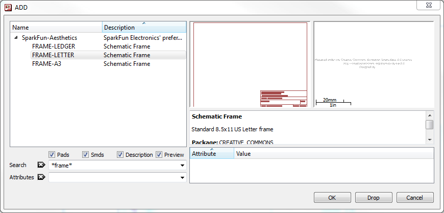
The frame isn't a critical component for what will be the final PCB layout, but it keeps your schematic looking clean and organized. The frame we want should be in the SparkFun-Aesthetics library, and it's named FRAME-LETTER. Find that by either searching or navigating and add it to your schematic.
After selecting the part you want to add, it'll âglowâ and start hovering around following your mouse cursor. To place the part, left-click (once!). Let's place the frame so its bottom-left corner runs right over our origin (the small dotted cross, in a static spot on the schematic).

After placing a part, the add tool will assume you want to add another: a new frame should start following your cursor. To get out of the add-mode either hit escape (ESC) twice or just select a different tool.
Right now your schematic is an untitled temporary file living in your computer's ether. To save either go to File > Save, or just click the blue floppy disk icon:  . Name your schematic something descriptive. How about âBareBonesArduino.schâ (SCH is the file format for all EAGLE schematics).
As a bonus, after saving, your frame's title should update accordingly (you may have to move around the screen, or go to View > Redraw).
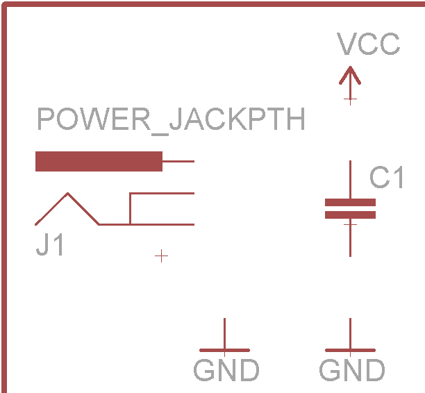
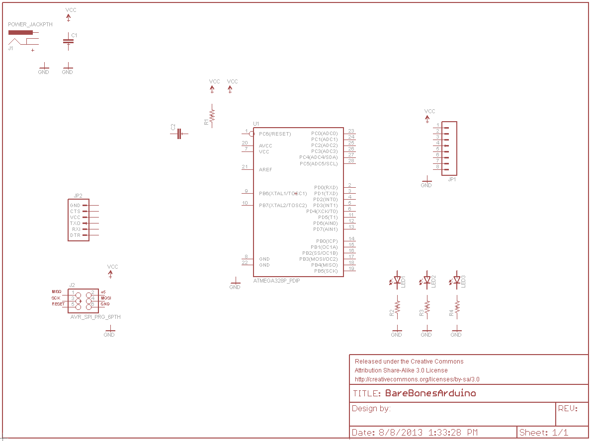
Next we'll add four different parts all devoted to our voltage supply input. Use the add tool for these parts:
| Part Description | Library | Part Name | Quantity |
|---|---|---|---|
| 5.5mm Barrel Jack (PTH) | SparkFun-Connectors | POWER_JACKPTH | 1 |
| 0.1µF Ceramic Capacitor | SparkFun-Capacitors | CAPPTH | 1 |
| Voltage Supply Symbol | SparkFun-Aesthetics | VCC | 1 |
| Ground Symbol | SparkFun-Aesthetics | GND | 2 |
All of these parts will go in the top-left of the schematic frame. Arranged like this:
If you need to move parts around, use the MOVE tool:  (left toolbar or under the Edit menu). Left-click once on a part to pick it up (your mouse should be hovering over the part's red â+â origin). Then left click again when it's where it needs to be.
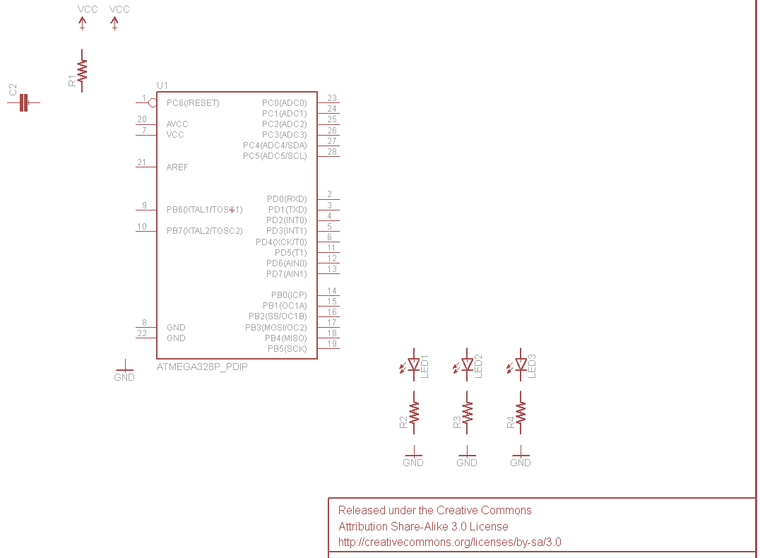
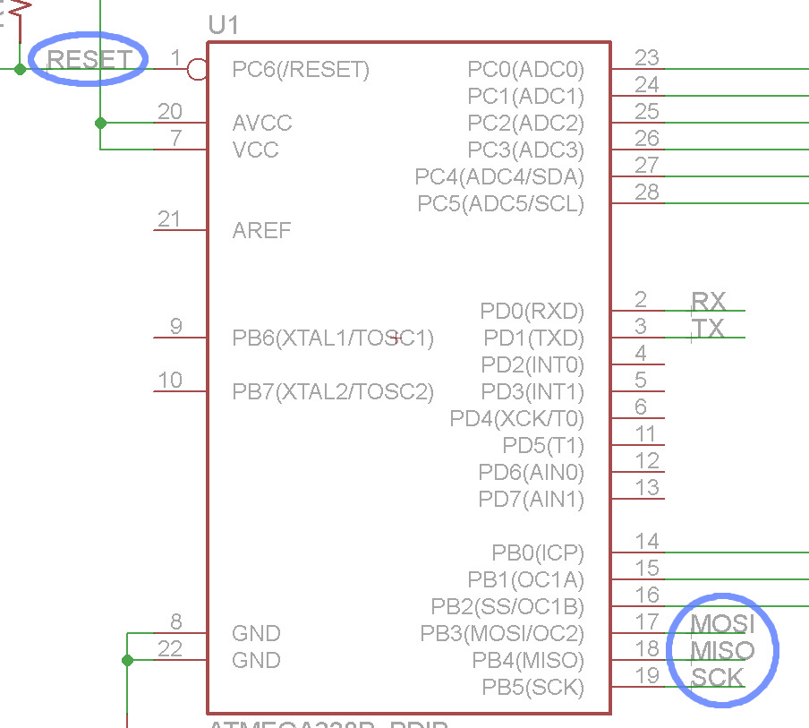
Next we'll add the main component of the design: the ATmega328 microprocessor: as well as some components to support it. Here are the parts we'll add:
| Part Description | Library | Exact Part Name | Quantity |
|---|---|---|---|
| ATmega328P (PTH) | SparkFun-DigitalIC | ATMEGA328P_PDIP | 1 |
| ¼W Resistors | SparkFun-Resistors | RESISTORPTH-1/4W | 4 |
| 5mm LEDs | SparkFun-LED | LED5MM | 3 |
| 0.1µF Ceramic Capacitor | SparkFun-Capacitors | CAPPTH | 1 |
| Voltage Supply Symbol | SparkFun-Aesthetics | VCC | 2 |
| Ground Symbol | SparkFun-Aesthetics | GND | 4 |
To rotate parts as your placing them, either select one of the four options on the rotate toolbar:  : or right click before placing the part. Place your microcontroller in the center of the frame, then add the other parts around it like so:
Three connectors will finish off our design. One 8-pin connector to break out the analog pins, a 6-pin serial programming header, and a 2x3-pin ICSP programming header. Here are the three parts to add for this step:
| Part Description | Library | Exact Part Name | Quantity |
|---|---|---|---|
| 8-Pin 0.1" Header | SparkFun-Connectors | M08 | 1 |
| 2x3 AVR Programming Header | SparkFun-Connectors | AVR_SPI_PRG_6PTH | 1 |
| 6-Pin Serial Programming Header | SparkFun-Connectors | ARDUINO_SERIAL_PROGRAMPTH | 1 |
| Voltage Supply Symbol | SparkFun-Aesthetics | VCC | 2 |
| Ground Symbol | SparkFun-Aesthetics | GND | 2 |
Finally! Here's what your schematic should look like with every part added:
Next we'll wire net them all together.
With all of the parts added to our schematic, it's time to wire them together. There's one major caveat here before we start: even though we're wiring parts on the schematic, we not going to use the WIRE tool:  : to connect them together. Instead, we'll use the NET tool:
  (left toolbar, or under the Draw menu). The WIRE tool would be better-named as a line-drawing tool, NET does a better job of connecting components.

To use the NET tool, hover over the very end of a pin (as close as possible, zoom in if you have to), and left-click once to start a wire. Now a green line should be following your mouse cursor around. To terminate the net, left-click on either another pin or a net.
The hard part, sometimes, is identifying which part on a circuit symbol is actually a pin. Usually they're recognizable by a thin, horizontal, red line off to the side of a part. Sometimes (not always) they're labeled with a pin number. Make sure you click on the very end of the pin when you start or finish a net route.
Start back in the upper left, and route the power input circuit like so:
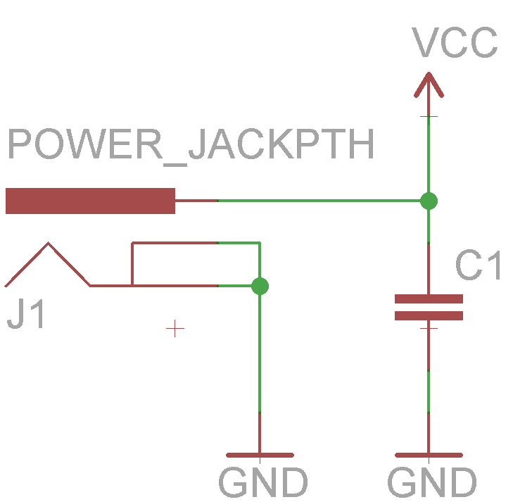
Whenever a net splits in two directions a junction node is created. This signifies that all three intersecting nets are connected. If two nets cross, but there's not a junction, those nets are not connected.
Next we'll route the ATmega328 to its supporting circuitry. There's LEDs, a connector, resistor, capacitor and VCC/GND symbols to route to:
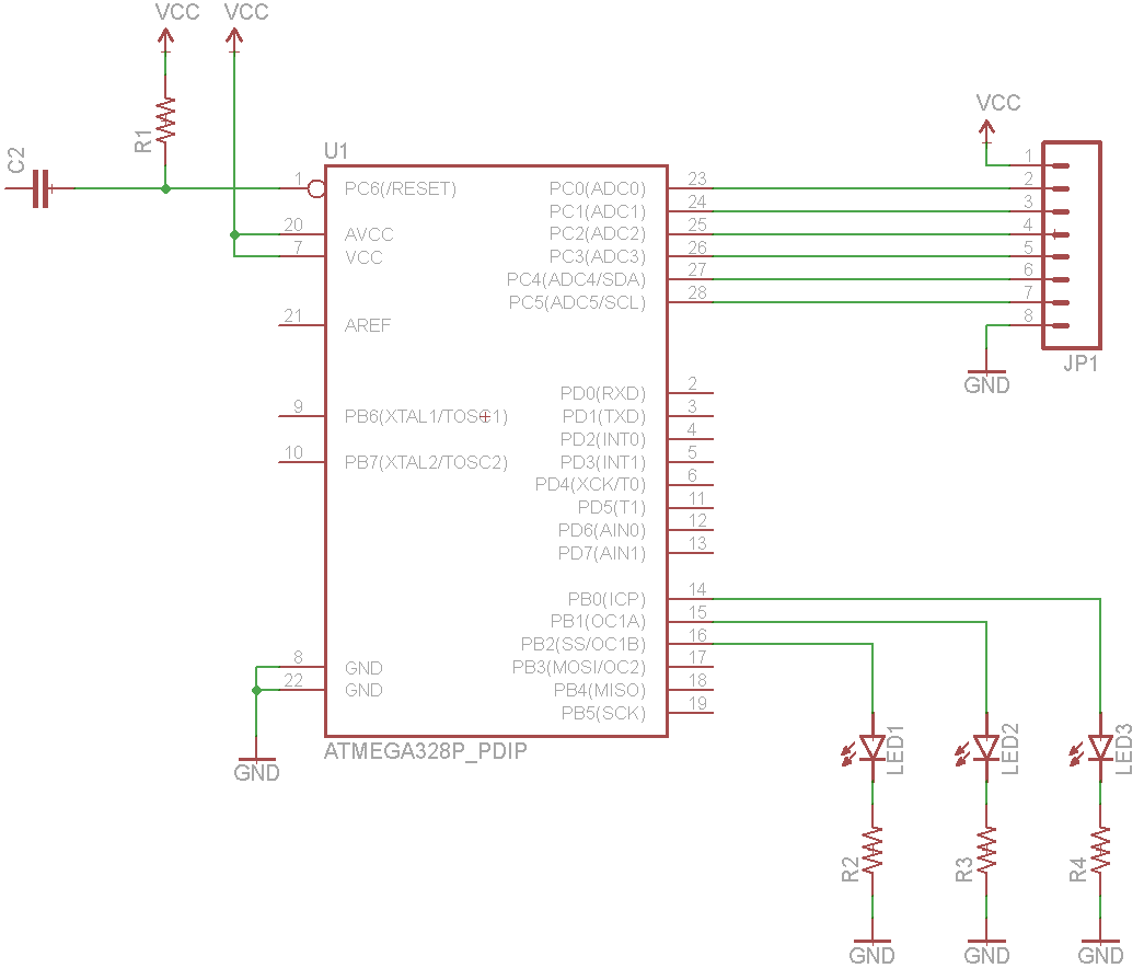
Don't forget to add nets between the LEDs, resistors, and GND symbols!
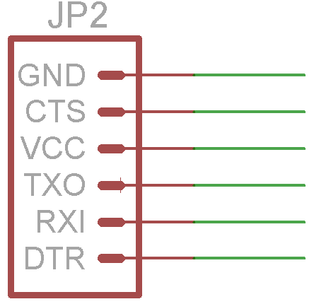
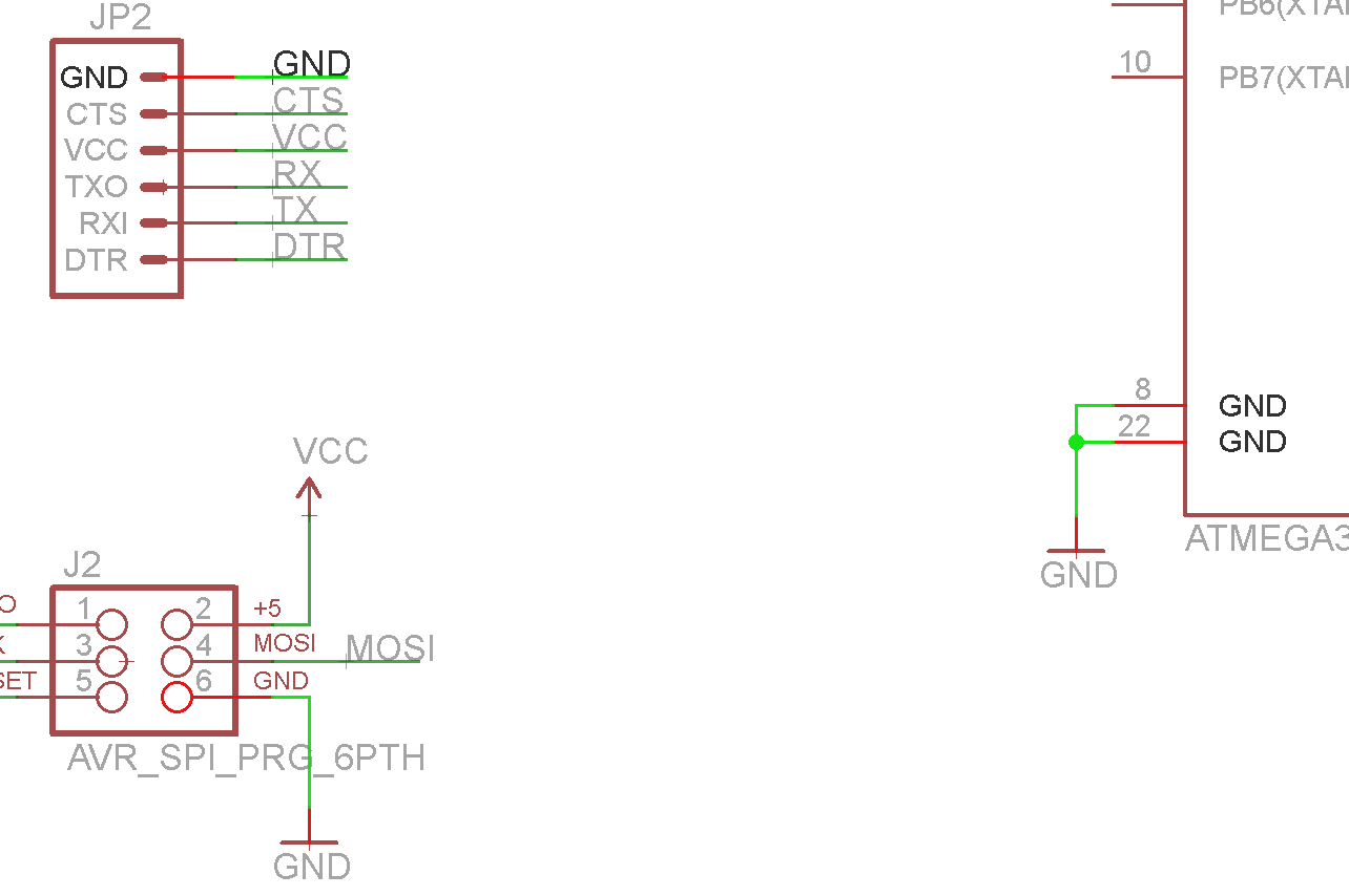
The remaining nets we have to make are not going to be as easy to cleanly route. For example, we need to connect the TXO pin on JP2 to the ATmega's RXD pin, all the way on the other side. You could do it, it would work, but it'd be really ugly. Instead, we'll make net âstubsâ and give them unique names to connect them.
We'll start by adding short, one-sided nets to each of the six pins on the serial connector. Begin by starting a net at a pin, just as you've been doing. Terminate the net by left-clicking a few grid-lengths over to the right of the pin. Then, instead of routing to another pin, just hit ESC to finish the route. When you're done, it should look like this:
Next, we'll use the NAME tool:  (left toolbar, or under the Edit menu): to name each of the six nets. With the NAME tool selected, clicking on a net should open a new dialog. Start by naming the net connected to the top, GND pin. Delete the auto-generated name (e.g. N$14), and replace it with âGNDâ (sans the quotation marks). This should result in a warning dialog, asking you if you want to connect this net to all of the other nets named âGNDâ (that would be every net connected to a GND symbol). Thanks for looking out for us EAGLE, but in this case Yes we do want to connect GND to GND.
After naming a net, you should use the LABEL tool:  : to add a text label. With the LABEL tool selected, left-click on the net you just named. This should spawn a piece of text that says âGNDâ, left-click again to place the label down right on top of your net.
Follow that same order of operations for the remaining five net stubs. In the end, they should look like this (note the net connected to the TXO pin is named âRXâ, and a âTXâ net connects to RXI: that's on purpose):
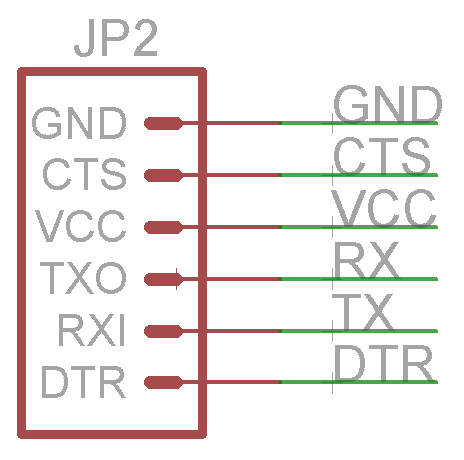
VCC should be the only other net that warns you that you'll be connecting to other nets named âVCCâ (anything connected to a VCC voltage node). For the other named nets, we'll need to create this same stub somewhere else. Where exactly? Well, we need to add a âRXâ and âTXâ net on the ATmega328, and a âDTRâ nearby as well:
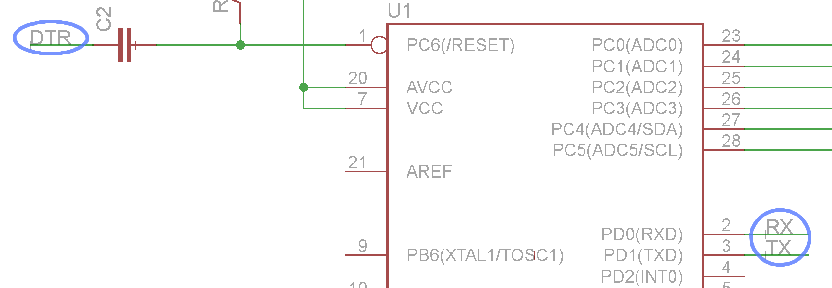
Even though there's no green net connecting these pins, every net with the same, exact name is actually connected.
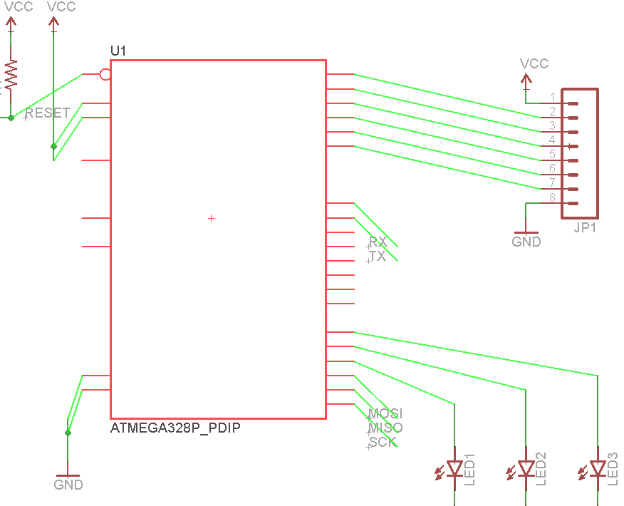
We need to do a lot of the same to connect the 2x3 programming header to the ATmega328. First, wire up the connector like so (naming/labeling MOSI, MISO, SCK, and RESET):
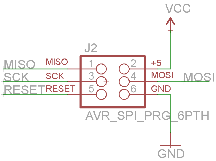
Then, back to the ATmega328, add the same four named/labeled nets:
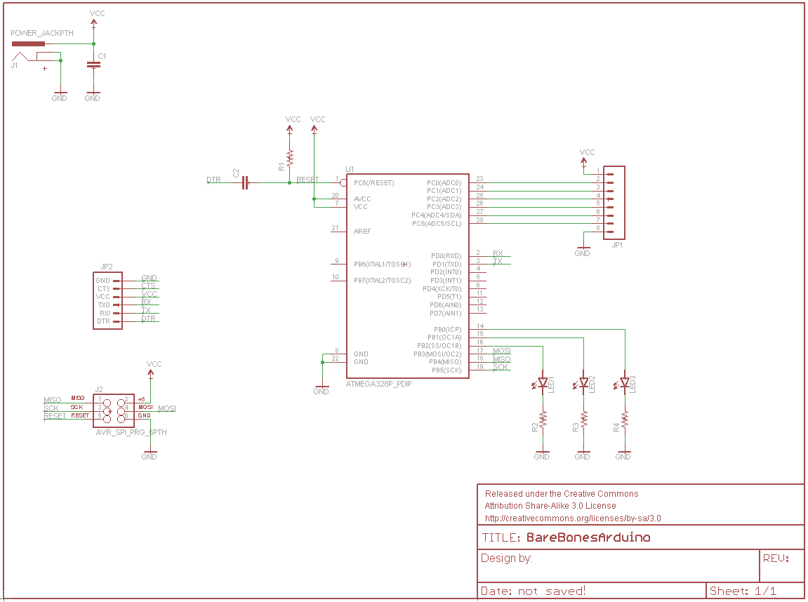
Phew: you're done. Get excited, it's about time to lay out a PCB! When your schematic is done, it should look a little something like this:
The schematic layout is done, but there are a few tips and tricks we'd like to share before moving over to the PCB layout portion of the tutorial.
Every component on your schematic should have two editable text fields: a name and a value. The name is an identifier like R1, R2, LED3, etc. Every component on the schematic should have a unique name. You can use the NAME tool: on any component to change the name.
A part's value allows you to define unique characteristics of that part. For example, you can set a resistor's resistance, or a capacitor's capacitance. The importance of a part's value depends on what type of component it is. For parts like resistors, capacitors, inductors, etc. the value is a critical piece of information when you're generating a bill of materials or assembly sheet. To adjust a part's value parameter, use the VALUE tool:  .
.
The SHOW tool:  : is very useful for verifying that pins across your schematic are connected correctly. If you use SHOW on a net, every pin it's connected to should light up. If you're dubious of the fact that two like-named nets are connected, give the SHOW tool a try. SHOW-ing a net connected to GND, for example, should result in a lot of GND nets lighting up.
As an alternative to show, you can temporarily MOVE a part a part to make sure nets are connected to it. Use MOVE to pick a part up, and the nets connected to it should bend and adjust to remain so. Just make sure you hit ESC to not move the part (or UNDO if you accidentally move it).
If all the nets connected to a part MOVE with it, all connections are good.
If a net isn't moving along with the part, it's not connected to the pin correctly. Double check to make sure you routed to the very end of the pin, and not a bit further:
If you have any nets incorrectly connected like above, DELETE:  : it, and try re-netting.
Any tool that you use on a single component, can also be used on a group of them. Grouping and performing an action on that group is a two-step process. First, use the group tool:  : to select the parts you want to modify. You can either hold down the left-mouse button and drag a box around them, or click multiple times to draw a polygon around a group. Once the group is made, every object in that group should glow.
After grouping, select the tool you want to use. The status box in the far bottom-left will have some helpful information pertaining to using the tool on a group:

In order to perform any action on a group, you have to select the tool, then hold down CTRL and right-click the group. After you CTRL+right-click, the tool will operate on the group just as it does a single component.
EAGLE's Copy :  : and Paste:
  : tools don't work exactly like other copy/paste tools you may have encountered before. Copy actually performs both a copy and paste when it's used. As soon as you copy a part (or any object on the schematic: name, text, net, etc.) an exact copy will instantly spawn and follow your mouse awaiting placement. This is useful if you need to add multiples of the same part (like GND nodes or resistors).
Paste can only be used to paste a group that has previously been copied to your clipboard. To use paste you first have to create a group, then (with the copy tool selected) CTRL+right-click to copy it, but hit ESC instead of gluing it down. This'll store the copied group into your operating system's clipboard, and you can use paste to place it somewhere. This tool is especially useful if you need to copy parts of one schematic file into another.
EAGLE's board designer is where a good portion of the magic happens. It's here where the dimensions of the board come together, parts are arranged, and connected by copper traces. In the board editor, the conceptual, idealized schematic you've designed becomes a precisely dimensioned and routed PCB.
In this tutorial we'll cover every step in EAGLE PCB design: from placing parts, to routing them, to generating gerber files to send to a fab house. We'll also go over the basics of EAGLE's board editor, beginning with explaining how the layers in EAGLE match up to the layers of a PCB.

The schematic from previous tutorial, complete with an ATmega328P, barrel jack connector, LEDs, resistors, capacitors, and connectors.
To switch from the schematic editor to the related board, simply click the Generate/Switch to Board command –  (on the top toolbar, or under the File menu) – which should prompt a new, board editor window to open. All of the parts you added from the schematic should be there, stacked on top of eachother, ready to be placed and routed.
The board and schematic editors share a few similarities, but, for the most part, they're completely different animals. On the next page, we'll look at the colored layers of the board editor, and see how they compare to the actual layers of a PCB.
PCB composition is all about layering one material over another. The thickest, middle part of the board is a insulating substrate (usually FR4). On either side of that is a thin layer of copper, where our electric signals pass through. To insulate and protect the copper layers, we cover them with a thin layer of lacquer-like soldermask, which is what gives the PCB color (green, red, blue, etc.). Finally, to top it all off, we add a layer of ink-like silkscreen, which can add text and logos to the PCB.
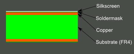
The layers of a double-sided PCB (image from the PCB Basics tutorial).
The EAGLE board designer has layers just like an actual PCB, and they overlap too. We use a palette of colors to represent the different layers. Here are the layers you'll be working with in the board designer. Note that the layers machined by the OtherMill are: Top, Bottom, Pad, Vias, Dimension and Holes.
| Color | Layer Name | Layer Number | Layer Purpose |
|---|---|---|---|
| Top | 1 | Top layer of copper | |
| Bottom | 16 | Bottom layer of copper | |
| Pads | 17 | Through-hole pads. Any part of the green circle is exposed copper on both top and bottom sides of the board. | |
| Vias | 18 | Vias. Smaller copper-filled drill holes used to route a signal from top to bottom side. These are usually covered over by soldermask. Also indicates copper on both layers. | |
| Unrouted | 19 | Airwires. Rubber-band-like lines that show which pads need to be connected. | |
| Dimension | 20 | Outline of the board. | |
| tPlace | 21 | Silkscreen printed on the top side of the board. | |
| bPlace | 22 | Silkscreen printed on the bottom side of the board. | |
| tOrigins | 23 | Top origins, which you click to move and manipulate an individual part. | |
| bOrigins | 24 | Origins for parts on the bottom side of the board. | |
| / / Hatch | tStop | 29 | Top stopmask. These define where soldermask should not be applied. |
| \ \ Hatch | bStop | 30 | Absent soldermask on the bottom side of the board. |
| Holes | 45 | Non-conducting (not a via or pad) holes. These are usually drill holes for stand-offs or for special part requirements. | |
| tDocu | 51 | Top documentation layer. Just for reference. This might show the outline of a part, or other useful information. |
To turn any layer off or on, click the "Layer Settings" button –  – and then click a layer's number to select or de-select it. Before you start routing, make sure the layers above (aside from tStop and bStop) are visible.
Here's one last tip before we get to laying our board out. This is an interface trick that trips a lot of people up. Since the board view is entirely two-dimensional, and different layers are bound to overlap, sometimes you have to do some finagling to select an object when there are others on top of it.
Normally, you use the mouse's left-click to select an object (whether it's a trace, via, part, etc.), but when there are two parts overlapping exactly where you're clicking, EAGLE doesn't know which one you want to pick up. In cases like that, EAGLE will pick one of the two overlapping objects, and ask if that's the one you want. If it is, you have to left-click again to confirm. If you were trying to grab one of the other overlapping objects, right-click to cycle to the next part. EAGLE's status box, in the very bottom-left of the window, provides some helpful information when you're trying to select a part.
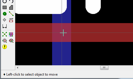
For example: In the GIF above, a VCC net overlaps another named Reset. We left-click once directly where they overlap, and EAGLE asks us if we meant to select VCC. We right-click to cycle, and it asks us instead if we'd like to select Reset. Right-clicking again cycles back to VCC, and a final left-click selects that as the net we want to move.
Whew! Enough pointers, let's lay out a PCB!
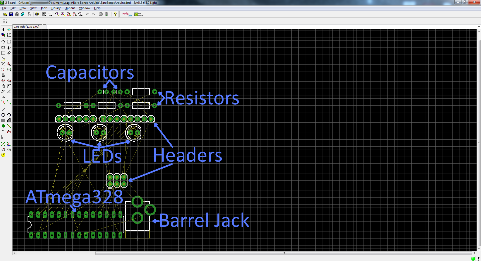
If you haven't already, click the Generate/Switch to Board icon – – in the schematic editor to create a new PCB design based on your schematic:
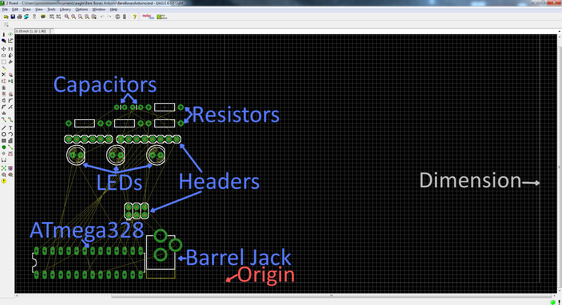
The new board file should show all of the parts from your schematic. The gold lines, called airwires, connect between pins and reflect the net connections you made on the schematic. There should also be a faint, light-gray outline of a board dimension to the right of all of the parts.
Our first job in this PCB layout will be arranging the parts, and then minimizing the area of our PCB dimension outline. PCB costs are usually related to the board size, so a smaller board is a cheaper board.
In the schematic editor we never even looked at the grid, but in the board editor it becomes much more important. The grid should be visible in the board editor. You can adjust the granularity of the grid, by clicking on the GRID icon –  . A 0.05" grid, and 0.005" alternate grid is a good size for this kind of board.

EAGLE forces your parts, traces, and other objects to "snap" to the grid defined in the Size box. If you need finer control, hold down ALT on your keyboard to access the alternate grid, which is defined in the Alt box.
Using the MOVE tool –  – you can start to move parts within the dimension box. While you're moving parts, you can rotate them by either right-clicking or changing the angle in the drop-down box near the top.
The way you arrange your parts has a huge impact on how easy or hard the next step will be. As you're moving, rotating, and placing parts, there are some factors you should take into consideration:
 – to get the airwires to recalculate.
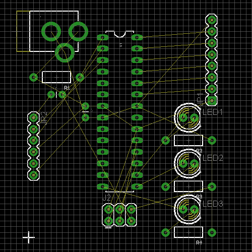
Below is an example of how you might lay out your board while considering those factors. We've minimized airwire intersections by cleverly placing the LEDs and their current-limiting resistors. Some parts are placed where they just have to go (the barrel jack, and decoupling capacitor). And the layout is relatively tight.
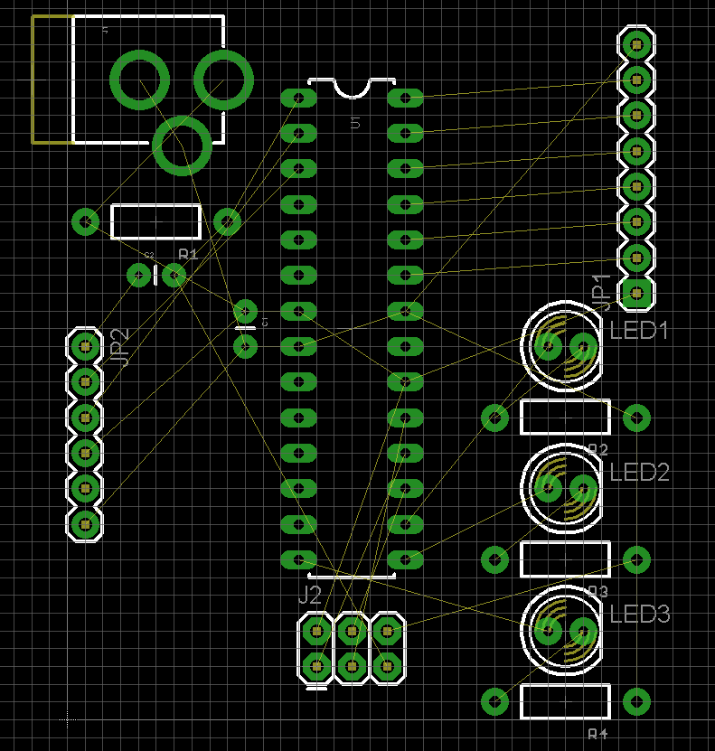
Note: The tNames layer (which isn't visible by default) was turned on to help identify which part is which.
Now that the parts are placed, we're starting to get a better idea of how the board will look. Now we just need to fix our dimension outline. You can either move the dimensions lines that are already there, or just start from scratch. Use the DELETE tool –  – to erase all four of the dimension lines.
Then use the WIRE tool – ( – to draw a new outline. Before you draw anything though, go up to the options bar and set the layer to 20 Dimension. Also up there, you may want to turn down the width a bit (we usually set it to 0.008").

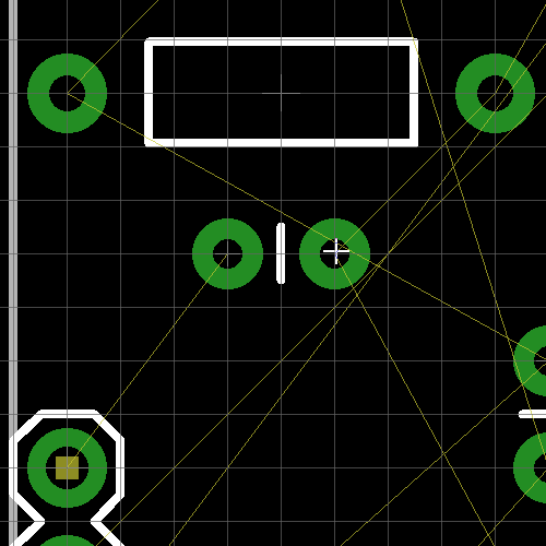
Then, starting at the origin, draw a box around your parts. Don't intersect the dimension layer with any holes, or they'll be cut off! Make sure you end where you started.
That's a fine start. With the parts laid out, and the dimension adjusted, we're ready to start routing some copper!
Routing is the most fun part of this entire process. It's like solving a puzzle! Our job will be turning each of those gold airwires into top or bottom copper traces. At the same time, you also have to make sure not to overlap two different signals.
To draw all of our copper traces, we'll use the ROUTE tool–  – (not the WIRE tool!). After selecting the tool, there are a few options to consider on the toolbar above:

With those all set, you start a route by left-clicking on a pin where an airwire terminates. The airwire, and connected pins will "glow", and a red or blue line will start on the pin. You finish the trace by left-clicking again on top of the other pin the airwire connects to. Between the pins, you can left-click as much as you need to "glue" a trace down.
While routing it's important to avoid two cases of overlap: copper over vias, and copper over copper. Remember that all of these copper traces are basically bare wire. If two signals overlap, they'll short out, and neither will do what it's supposed to.
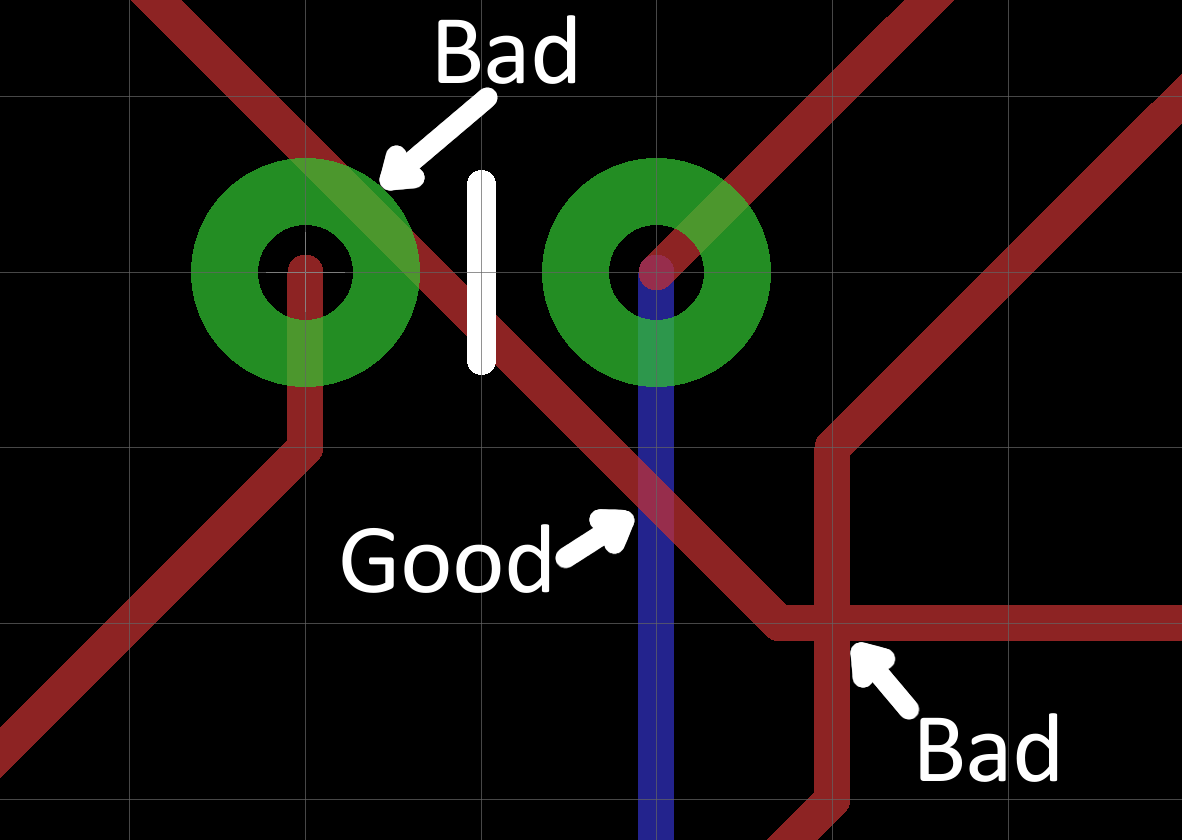
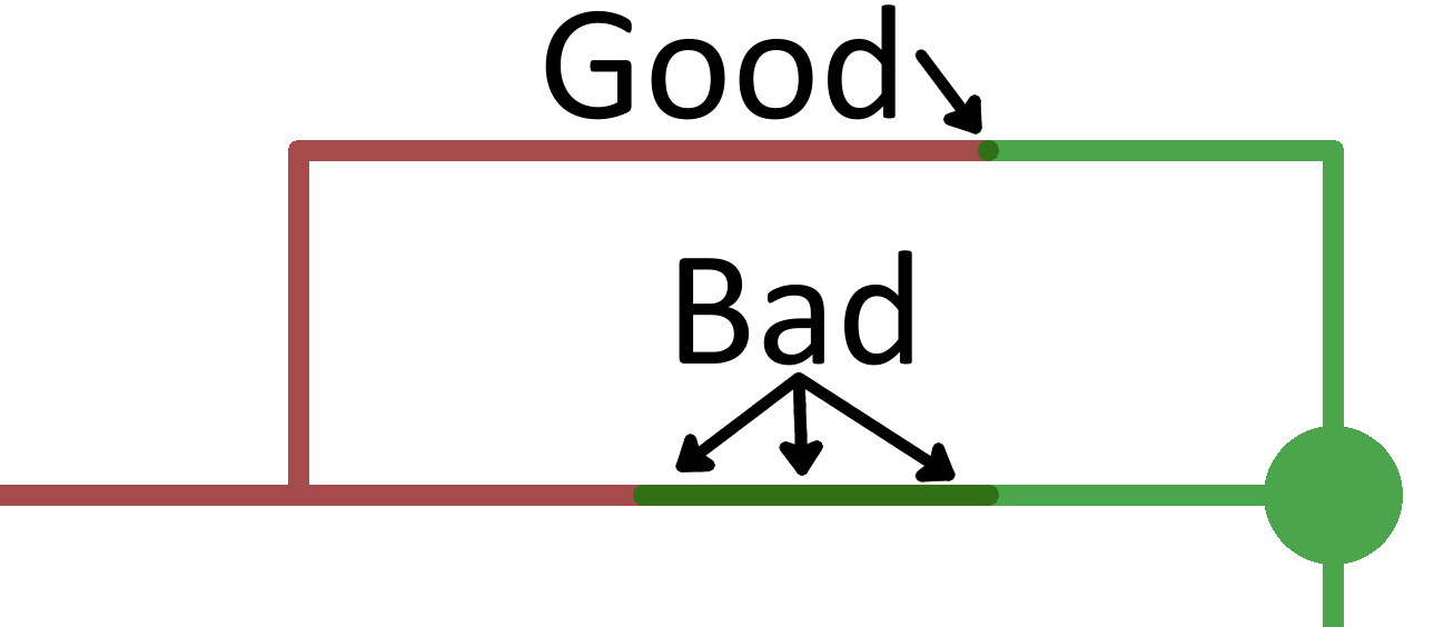
If traces do cross each other, make sure they do so on opposite sides of the board. It's perfectly acceptable for a trace on the top side to intersect with one on the bottom. That's why there are two layers!
If you need more precise control over your routes, you can hold down the ALT key on your keyboard to access the alternate grid. By default, this is set to be a much more fine 0.005".
Vias are really tiny drill holes that are filled with copper. We use them mid-route to move a trace from one side of the board to the other.
To place a via mid-route, first left-click in the black ether between pins to "glue" your trace down. Then you can either change the layer manually in the options bar up top, or click your middle mouse button to swap sides. And continue routing to your destination. EAGLE will automatically add a via for you.
Make sure you leave enough space between two different signal traces. PCB fabricators should have clearly defied minimum widths that they'll allow between traces – probably around 0.006" for standard boards. As a good rule-of-thumb, if you don't have enough space between two traces to fit another (not saying you should), they're too close together.
Much like the WIRE tool isn't actually used to make wires, the DELETE tool can't actually be used to delete traces. If you need to go back and re-work a route, use the RIPUP tool –  – to remove traces. This tool turns routed traces back into airwires.
You can also use UNDO and REDO to back/forward-track.
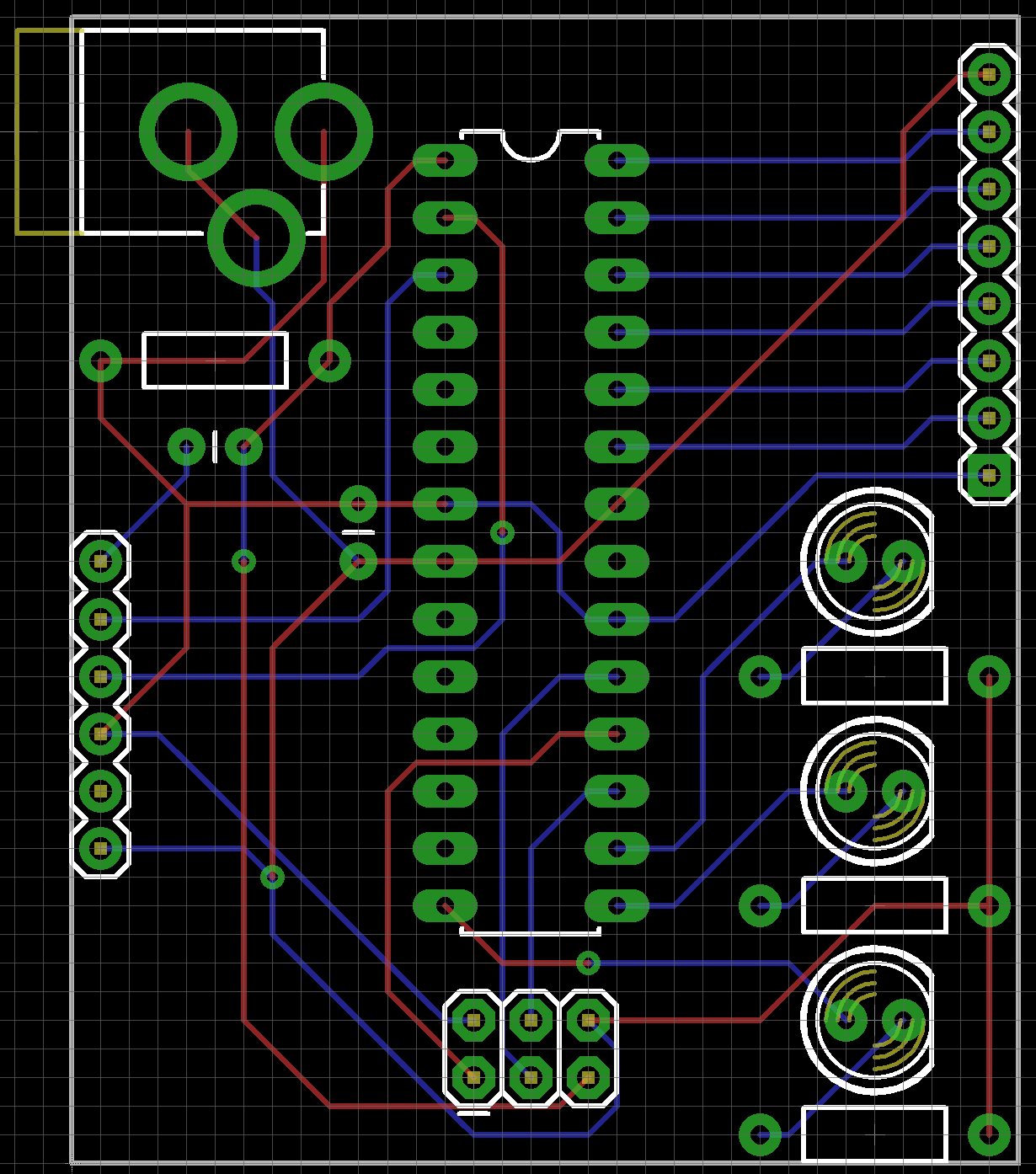
That's about all the simple rules there are. Go have the time of your life solving the routing puzzle! You may want to start on the closest, easiest traces first. Or, you might want to route the important signals – like power and ground – first. Here's an example of a fully-routed board:
See if you can do a better job than that! Make your board smaller. Or try to avoid using any vias.
After you feel like the routing is done, there are a few checks we can do to make sure it's 100% complete. We'll cover those on the next page.
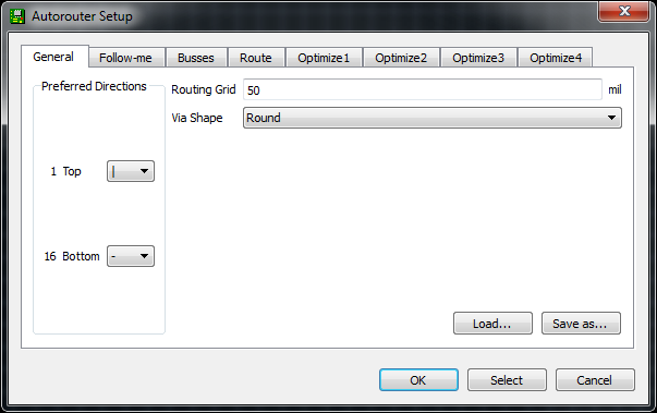
If you're short on time, or having trouble solving the routing puzzle, you can try loading up EAGLE's Autorouter –  – to see if it can finish the job. Open up the autorouter, don't worry about these other tabs for now, just click OK.
If you don't like the job the autorouter did, you can quickly hit Undo to go back to where you were.
The autorouter won't always be able to finish the job, so it's still important to understand how to manually route pads (plus manual routes look much better). After running the autorouter, check the bottom-left status box to see how it did. If it says anything other than "OptimizeN: 100% finished", you've still got some work to do. If your autorouter couldn't finish the job, try turning Routing Grid down from 50mil 10mil.
There are tons of optimizations and settings to be made in the autorouter. If you want to dig deeper into the subject, consider checking out EAGLE's manual where an entire chapter is devoted to it.
Before we package the design up and send it off to the fabrication house, there are a few tools we can use to check our design for errors.
The first check is to make sure you've actually routed all of the nets in your schematic. To do this, hit the RATSNEST icon – – and then immediately check the bottom left status box. If you've routed everything, it should say "Ratsnest: Nothing to do!"

As denoted by the exclamation mark, having "nothing to do" is very exciting. It means you've made every route required.
If ratsnest says you have "N airwires" left to route, double check your board for any floating golden lines and route them up. If you've looked all over, and can't find the suspect airwire, try turning off every layer except 19 Unrouted.
Once you're done routing there's just one more check to be made: the design rule check (DRC). For this step, we recommend you use the Other Machine Co. design rules, which you can download here. Select the design rule corresponding to the endmill being used (1/32" or 1/64" Flat Endmill). To load up the DRC, click the DRC icon –  – which opens up this dialog:
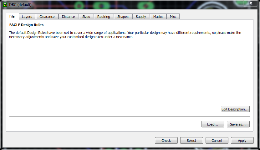
The tabs in this view (Layers, Clearance, Distance, etc.) help define a huge set of design rules which your layout needs to pass. These rules define things like minimum clearance distances, or trace widths, or drill hole sizes, all sorts of fun stuff. Instead of setting each of those manually, you can load up a set of design rules using a DRU file. To do this, hit Load and select the .dru file you just downloaded. The title of the window will change to "DRC (Othermill-DRC-1-32)", and some values on the other tabs will change. Then hit the Apply button and finally the Check button.
Again, look down to the bottom-left of the editor. If your design is perfect, you should see "DRC: No errors." But if things didn't go so swell, you'll instead be greeted by the dreaded "DRC Errors" window. The error window lists all of the open errors, and it also highlights where the error is. Click on any of the errors listed, and EAGLE will point to the offender.
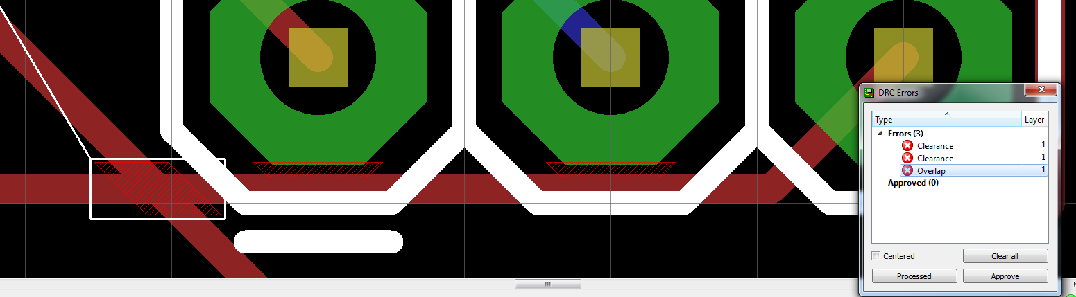
There are all sorts of errors that the DRC can find, but here are some of the most common:
Once you've seen both "No airwires left!" and "DRC: No errors." your board is ready to send to the fab house.