|
Art of Science 2013 Online Gallery
«Prev |
Thumbnails |
Next »
|
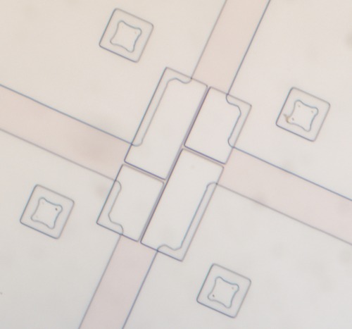 Conducting path
Chiao-Ti Huang (graduate student)
Department of Electrical Engineering
I created this complicated pattern in silicon by etching away most of the electrically conducting regions, leaving eight pathways (the pinkish stripes) for electrons to flow. The big pathways are 10 microns across. The narrow paths (center of image) are only 1/20th that width. This research helps us better understand how electrons flow through semiconductors.
As electrons flow through this device they can suddenly find themselves on a narrow road where they have to "decide" to go left or right, not "knowing" where to head. This is not unlike what happens to people on the road of life. Suddenly you realize you are walking on a narrow trail that seems to have no clear direction. Go ahead? Turn right or left? You must make your decision bravely and hope this narrow trail will ultimately connect you to another, better world.
|
|