Facilities
The Ceramic Materials Laboratory (CML) facilities are roughly divided into two categories, Characterization and Processing. All facilities are located in rooms A001-007, G102, G104, and G106 of the Engineering Quadrangle (or EQuad), home of the School of Engineering and Applied Sciences. The A-Wing of the EQuad (Hayes Hall) is the home of the CML's parent department, the Department of Chemical and Biological Engineering. The G-Wing facilities have been extensively remodeled to facilitate characterization and synthesis instrumentation.
The central topic guiding research within the CML is implied by its name, the processing and characteristics of ceramic-matrix materials. During the past decade, a notable shift towards nanoscale processing through self-assembly has defined the research task areas and projects within the group. Descriptions of our research activities can be found on our Research web page along with short descriptions of the funded projects within our group.
The following text and pictures give a virtual tour of our facilities, highlighting our equipment and the respective applications of each. But it should be noted that these represent only those instruments and equipment that are contained within our laboratories. CML members also have access to advanced imaging instrumentation within the Imaging and Analysis Center (IAC) of the Princeton Institute for the Science and Technology of Materials (PRISM) Central Facilities.
Characterization
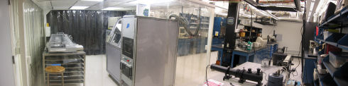
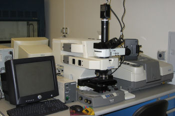
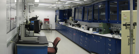
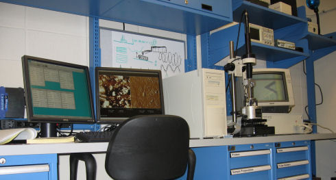
Characterization and Testing Laboratory, Room G106 .
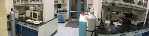
Our Characterization and Light Processing Facilities, mostly located in Rooms G102 through G106 of the EQuad, consist of several modern laboratories built on a configurable floor plan to maximize utility and provide for future research needs. These laboratories contain a mix of bench and floor mounted equipment, most of which would be familiar to materials scientists.
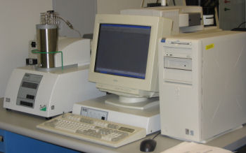
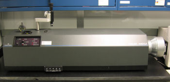
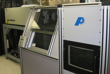
Netzsch 449C Jupiter TG-DSC.
Three key methods in thermal analysis are Differential Scanning Calorimetry (DSC), Thermogravimetric Analysis (TGA), and Dilatometry. Our Netzsch Jupiter combines simultaneous DSC and TGA on a single sample covering the temperature range from -120°C to 1650°C. The change in sample weight is continuously monitored with respect to temperature. Additionally, enthalpic measurements can be validated for melting point, glass transition, phase changes, and crystallization with no observed weight loss. An outlet port from the sample chamber permits the TG-DSC unit to be coupled to an FTIR spectrophotometer for evolved gas analysis (EGA), identifying the products of heat treatment.
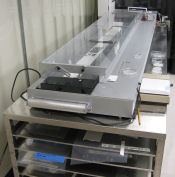
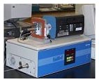 The
Orton dilatometer (left) measures dimensional changes of materials during
heating or cooling of the sample. Both reversible and irreversible changes in
the length of a specimen can be measured. Typically, this is done with a ceramic
push rod in direct contact with the specimen. Dilatometry can pinpoint where
dimensional changes occur, knowledge of which is important because expansion or
contraction in a material creates stresses that can cause cracking. Dimensional
determinations include: expansion coefficient; softening point; glass transition
temperature, Curie point; crystalline transformation; phase transition;
shrinkage; bloating; sintering rate; isothermal creep; and stress relaxation.
The
Orton dilatometer (left) measures dimensional changes of materials during
heating or cooling of the sample. Both reversible and irreversible changes in
the length of a specimen can be measured. Typically, this is done with a ceramic
push rod in direct contact with the specimen. Dilatometry can pinpoint where
dimensional changes occur, knowledge of which is important because expansion or
contraction in a material creates stresses that can cause cracking. Dimensional
determinations include: expansion coefficient; softening point; glass transition
temperature, Curie point; crystalline transformation; phase transition;
shrinkage; bloating; sintering rate; isothermal creep; and stress relaxation.
Thermo Electron Nexus 670 FTIR with Continuµm IR microscope.
Our spectroscopy facility includes both FTIR and UV/Visible spectroscopy in addition to X-ray diffractometry for the analysis of materials. Infrared microscopy (15µm resolution) is provided by the Continuµm IR microscope. The infrared adsorption of a sample provides chemical information about the sample and the infrared fingerprint aids in the identification of unknowns in all states of matter: vapor, liquid, and solid and can be used to characterize interfacial interactions such as surfactant adsorption. X-ray diffractometry (XRD) is provided by the Rigaku Miniflex diffractometer, a bench top unit that provides qualitative and quantitative identification of crystalline phases. Coupled with analytical software, unknown crystalline materials can be readily identified.
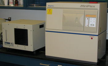
Rigaku MiniFlex X-ray diffractometer.
An important component of nanoscale characterization is laser light scattering. Light is scattered by polarizable particles in a sample. The oscillating electric field in the beam of light induces oscillating dipoles in the particles, radiating light in all directions. This phenomenon is used to measure particle size (~3 nm to 1µm), molecular weight, shape, diffusion coefficients and so on. Our unit provides both Static Light Scattering (SLS) and Dynamic Light Scattering (DLS). In the SLS mode time-averaged intensity measurements are made at either fixed or variable angles in the range from 80 to 155°. DLS, from the rapid thermal (Brownian) motions of the particles, is also used to measure particle size distributions and to chart the kinetics of precipitation, growth, and diminution.
Brookhaven Instruments Corp. goniometer and laser light scattering system.
Electrokinetics Laboratory, Room G102A .
Additional particle characterization is provided by the Coulter 440SX Doppler electrophoretic light scattering analyzer (DELSA), used to measure the electrophoretic mobility distribution, zeta potential, specific conductivity and average hydrodynamic radius of particles in liquid suspensions. The particles can be either solid or liquid within the size range of 10nm to 30µm. The system analyses the particles by making simultaneous independent doppler measurements at four different angles, each with a 256-channel resolution. This allows the detection of very small particles as well as the separation effects due to electrophoretic inhomogeneity, thermal diffusion and flow inhomogeneity. The unit is housed in a constant temperature room to minimize thermal fluctuations during sampling.
Coulter DELSA 440SX.
Rheometers are used to characterize viscoelastic properties of suspensions and solutions. The Rheometric Scientific RFS II is used in diverse applications, ranging from studying the texture and flow of ceramic powder suspensions, measuring the fluidity of photocurable polymers, to measuring the stiffness and stability of ceramic/polymer composites.
Rheometrics RFS II fluids spectrometer.
The surface area and channel characteristics (especially accessibility, uniformity, and continuity) are essential to the efficient design and use of catalytic and sensor support matrices. The Micromeritics Gemini surface analyzer provides researchers with the basic tools for structural analysis of micro- and nanoporous materials. Increased interest in the use of self-assembled surfactants, oligomers, and polymeric systems to build such materials through co-assembly or templation of inorganic precursors requires details of structure that can be revealed via surface sorption of gas or vapor.
Micromeritics Gemini 2380 Surface Area Analyzer
Microscopy
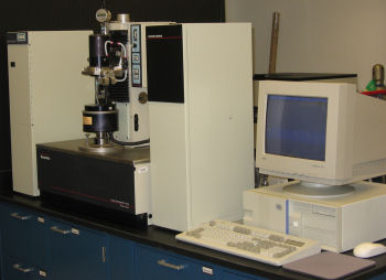
Extensive microscopy facilities exist within the CML, including optical microscopy (OM), Brewster angle microscopy (BAM), scanning electron microscopy (SEM), and atomic force microscopy (AFM). The AFM especially is a centerpiece of the characterization resources, providing atomic scale imaging on surfaces under air or liquid.
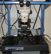
Electrokinetics and Microscopy Laboratory, Room G102B.
The AFM probes the surface of a sample by rastering across the surface with a sharp tip, a few microns long and often less than 100Å in diameter. AFM imaging can be done at the atomic scale on well-ordered samples and under fluid. Contact mode AFM involves contacting the tip to the sample surface while non-contact mode keeps the tip off the surface, using only the force between the tip and the surface to create the necessary deflection. Sample applications within our group include imaging self-assembled surfactant molecules and biological molecules (e.g., DNA and proteins) on different substrates. The AFM laboratory is maintained in our basement facility in room A002.
AFM Laboratory, Room A002, housing the Veeco Digital Instruments Nanoscope IIIA.
 The quest for miniaturized components fabricated from piezoelectric materials to emulate and surpass silicon-based
structures (such as the most common MEMS devices) requires characterization tools that are capable of measuring very small
fields. The Sigatone Probe Station allows the direct measurement of piezo- and ferroelectric response in milli- and microscale
devices such as the PZT micro-cantilevers under investigation. Our ferroelectric test station is housed in A002 EQuad, along
with the AFM allowing the two instruments to be linked in the analysis of responsive ceramic structures.
The quest for miniaturized components fabricated from piezoelectric materials to emulate and surpass silicon-based
structures (such as the most common MEMS devices) requires characterization tools that are capable of measuring very small
fields. The Sigatone Probe Station allows the direct measurement of piezo- and ferroelectric response in milli- and microscale
devices such as the PZT micro-cantilevers under investigation. Our ferroelectric test station is housed in A002 EQuad, along
with the AFM allowing the two instruments to be linked in the analysis of responsive ceramic structures.
Somewhat akin to the AFM, the Scanning Vibrating Probe (SVP) operates with a non-intrusive scanning, vibrating probe measuring and mapping the electric field generated in a plane above the surface of an electrochemically active sample. This enables local electrochemical and corrosion events to be mapped in real time. The Scanning Kelvin Probe (SKP) is a non-contact, non-destructive instrument designed to measure the surface work function difference between conducting, coated, or semi-conducting materials and a metallic probe. The technique operates using a vibrating capacitance probe, and through a swept backing potential, the work function difference is measured between the scanning probe reference tip and sample surface. The work function can be directly correlated to the surface condition. A unique aspect of the SKP is its ability to make measurements in a humid or gaseous environment. The utility of SVP and SKP are combined in a single instrument, the Uniscan M370 electrometer in our G102A Laboratory.
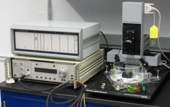
The Uniscan (UK) M370 SVP/SKP in G102A Laboratory.
Brewster angle microscopy (BAM) permits the direct observation of ultrathin organic films on transparent dielectric substrates. It is based on the effect that from the clean surface no reflection occurs when p-polarized incoming light under the Brewster angle. The "black background" of the Brewster Angle setup allows using a detector (typically a CCD-camera) at maximum intensity. A very thin organic layer (e.g., a 2nm thick monolayer) with different refractive index will cause reflection. The resulting reflection is only about a millionth of the incident intensity. The reflected light can be used to form a high contrast image of the lateral morphology of the layer.
The Nanofilm BAM in the G102B Laboratory.
The Tescan SEM is comparatively low resolution (20-100nm) electron microscope that is used for providing electron micrographs of sample surfaces in 3-dimensions. If higher resolution or lower accelerating voltage is required for a particular sample, the Tescan SEM allows the user to preview his/her sample before using a higher resolution instrument, such as the FEI XL30 FEG-SEM housed in PRISM.
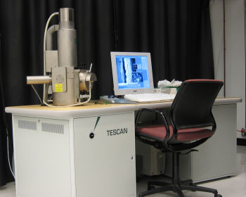
Tescan Vega SEM in G106 Laboratory.
Additional optical microscopy is provided by the Leitz Metallovert, used for metallographic imaging of polished and etched surfaces; the Zeiss Axioplan 2 imaging microscope, used for dynamic studies on particle organization under applied and static fields; and the Mitutoyo imaging microscope, useful for large area optical scans.
Optical microscopes in the CML Laboratories. (Left) The Zeiss microscope in the foreground is used to image particle movement and organization under an applied field. The Leitz Metallograph in the background is used for metallographic analysis of etched surfaces. (Right) The Mitutoyo OM is a large area panning microscope, often used for lower magnification of patterned surfaces.
Materials Processing Facilities
Stereolithography and Patterning
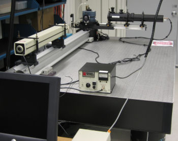
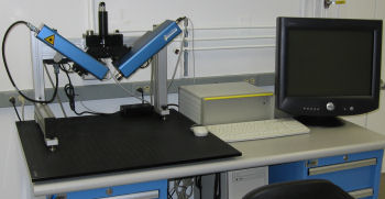
In electrohydrodynamic printing (EHDP), we utilize the cone-jet transition in a stream from a millimeter-sized nozzle to produce micrometer-scale charged jets of fluid. EHDP uses these charged jets like a liquid micro-pen to pattern surfaces on the micro- to nanometer scale. Small feature sizes (down to ~100 nm) resulting from both the cone-jet transition and stretching of the deposited fluid stream, permits accurate deployment of nanofibers. The stream stability and rapid feed rate due to the jet's high velocity make EHDP advantageous over current direct printing techniques in several different aspects. Our assembled system provides the necessary stability and control over the feed and jet. Patterning is currently limited by the available mechanics, but the acquisition of an air-bearing, magnetically controlled patterning bed will allow the construction of more complicated patterns using EHDP.
EHDP bench in the Electrohydrodynamics Laboratory, Room G104B.
Ceramic, polymer, and ceramic/polymer composite parts can be fabricated using three-dimensional stereolithography. This process starts with the design of the part to be made as a three-dimensional virtual solid using a computer aided design program. The solid is then rendered into thin virtual slices (0.075 mm thick) along the z-axis; this stack of layers is used for fabricating the part. The solid object is constructed layer-by-layer: first replicating a layer by raster scanning an UV laser across the surface of a photocurable resin bath, covering the cured layer with fresh resin, and repeating the patterning to form the next layer. The cycle is repeated until the entire object has been built. Our work uses the resin as the medium for a highly concentrated colloidal suspension. A ceramic green body is the result.

The 3D Systems SLA250 stereolithography unit builds 3-dimensional objects by layering 2-dimensional "slices" of a CAD design, using photocurable resin as the matrix.
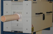
Laser drilling has found successful manufacturing applications in the aerospace, automotive, energy, electronics, medical, pharmaceutical, and consumer goods industries. Lasers make it possible to machine very small holes, unusual-shaped holes, blind holes, and precisely tapered holes. Laser drilling is also used to drill holes at steep angles, and to process difficult-to-machine materials. A single setup can produce hundreds of different sizes over a 3-D surface. In our laboratory, coupling a 60W cutting laser (the PulseMaster PM800) with a precision patterning base and control unit permits the patterning of ceramic tapes with precisely drilled holes. Layering these patterned tapes results in a laminated structure that resembles the gross structural morphology of seashells.
The PulseMaster PM800 cutting laser with control unit and patterning chamber.
 The Mettler tape caster
is used to form large area, thin, and flat ceramic tapes, its chief advantage as
these are virtually impossible to press and most difficult if not impossible to
extrude. Punching or drilling holes and slots of various sizes and shapes into
unfired tape is relatively easy and is essential to the multilayered ceramic
composites of interest to our group, such as seashell-type strurctures. The thin
ceramic sheets are essentially two dimensional structures since they are large
in the x and y directions and very thin in the z dimension (12µm to 3mm). To
minimize contamination from dust or other particulates, tape casting is done
within a Class 100 clean bay.
The Mettler tape caster
is used to form large area, thin, and flat ceramic tapes, its chief advantage as
these are virtually impossible to press and most difficult if not impossible to
extrude. Punching or drilling holes and slots of various sizes and shapes into
unfired tape is relatively easy and is essential to the multilayered ceramic
composites of interest to our group, such as seashell-type strurctures. The thin
ceramic sheets are essentially two dimensional structures since they are large
in the x and y directions and very thin in the z dimension (12µm to 3mm). To
minimize contamination from dust or other particulates, tape casting is done
within a Class 100 clean bay.
Wet Chemistry
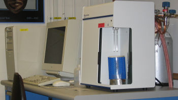
Chemistry Laboratory, Room A004.
Our A001 EQuad laboratory complex is the location of the wet chemistry laboratory, dedicated to solvent-based processing, where ceramic suspensions and templated complex fluids are prepared. A controlled atmosphere Dritrain and standard fume hoods (not shown) are provided for dealing with volatiles and environmentally sensitive precursors. Equipment located here includes pH meters, a high energy ultrasonicator (often used for breaking up powder agglomerates in suspensions), and a de-airing station for removing air from suspensions. Ashing furnaces for burning out polymers and binders from consolidated green compacts are located in the requisite fume hood.
Supercritical Extraction
The use of organic structure-directing agents, whether templates or agents of co-assembly, typically requires the removal of the organic component following the conversion of the inorganic precursor to the structured ceramic. The differential pressures that can arise within the porous body during normal or high temperature drying can be eliminated through the use of supercritical solvent extraction. In our laboratory, we use either carbon dioxide extraction, normally used for making silica aerogels, or organic solvent extraction. The latter, although requiring higher critical pressures and temperatures, is usually more effective at removing organic materials due to higher solubility with the extracting solvent.
(Left) Supercritical CO2 extractor. (Right) Supercritical organic solvent extraction system.
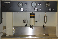
High Temperature Processing
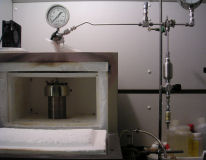
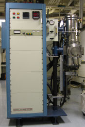
Thermal Processing Laboratory, Room A006, showing sintering furnace (left), high temperature/high pressure reaction chamber (center), and vacuum drying oven (far right).
 |
As a ceramic materials group, it is not surprising that we have high temperature processing capabilities. The furnaces range from simple box furnaces, vertically and horizontally mounted tube furnaces (left), and very high temperature (up to 3,000°C) vacuum furnaces. These units are all located in the A001 complex of laboratories within the A-Wing of the EQuad. |
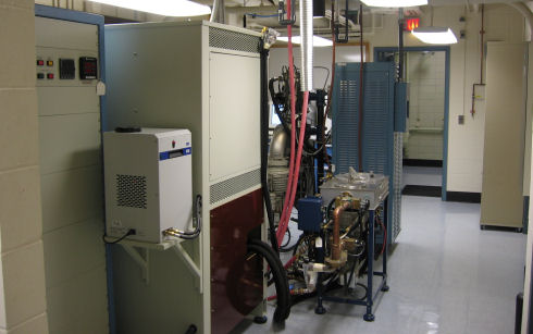
High Temperature Furnace Laboratory, Room A001, containing the Thermal Technology Brew (foreground) and Astro (background) furnaces.
 |
The CML has 1700°C Lindbergh box furnaces for sintering in air, an Astro 2500°C (left) graphite furnace for sintering non-oxides in both inert atmospheres and vacuum, and a 2000°C Brew furnace, a vacuum furnace with tantalum radiation shielding primarily used for infiltrating porous ceramic compacts with liquid metals. The Astro and Brew furnaces are now covered by Thermal Technology. Horizontal mount tube furnaces are used in the processing of graphene sheets while the vertical mount tube furnaces have been used for growing single crystal yttrium barium copper oxide (123) superconducting single crystals. |
Powder Synthesis and Consolidation
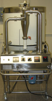 The Niro spray dryer
(right) is used for the processing of ceramic powders
from organometallic precursors, and offers the best method for controlling
particle size and morphology. The dried precursor often contains nitrates and
other fuels so that the dried powder is fed directly into a hot tube furnace for
combustion to an oxide phase.
The Niro spray dryer
(right) is used for the processing of ceramic powders
from organometallic precursors, and offers the best method for controlling
particle size and morphology. The dried precursor often contains nitrates and
other fuels so that the dried powder is fed directly into a hot tube furnace for
combustion to an oxide phase.
Powder consolidation is a traditional method for improving the packing of ceramic powder compacts, thereby reducing sintering temperature and times while simultaneously reducing void volume and size distribution. Our cold isostatic press (CIP, not shown) compacts the powder under hydrostatic pressure under ambient conditions to achieve this. However, within the CML it is regarded as a method of last resort. Our research into colloidal particle processing seeks to avoid such high energy processes such as the CIP and its complementary technique, the hot isostatic press (HIP) which combines high pressure with high temperatures.
![]()
![]()
![]() ©
Princeton University, Department of Chemical and Biological Engineering
©
Princeton University, Department of Chemical and Biological Engineering
Ceramic Materials Laboratory. All Rights Reserved.