Research: Hierarchically Structured Self-Assembled Materials
Anthony Y. Ku
Advisors: Dudley A. Saville and Ilhan A. Aksay
Hierarchically structured materials possess structural organization at multiple length scales. [1] Appropriate organization of the structure leads to enhanced material properties and performance. Many naturally occurring biomaterials are hierarchically ordered. For example, both bone and mother-of-pearl nacre (materials that are of present interest to this group) possess functional structure from centimeter to nanometer lengths. [2] Complex synthetic processes are needed to prepare simple artificial versions of these materials; biomaterials self assemble at each of the length scales naturally.
Our hierarchically structured self-assembled materials effort is interested in composite materials that possess hierarchical structure and self assemble at the appropriate length scales. We seek to develop general methods for producing synthetic hierarchically ordered composite materials. In particular, we are working on exploit the self-assembly tendencies of amphiphilic organic molecules to generate structure at the nanometer length scale and induce pattern formation using field effects at the micron length scale. We are also working towards developing models for understanding the synthesis and behavior of these materials.
We have chosen mesoscopic silica as a model system for our work. Discovered in 1992 by scientists at Mobil [3], this material possesses order at both the micron and nanometer length scales (below). This material is prepared by combining sol-gel chemistry with organic templating agents. The organic templating agents (typically amphiphilic surfactants or block copolymers) self-organize at the nanometer length scale to form the monodisperse, well-packed channels. The size and packing of the channels is determined by the identity of the organic species. [4]
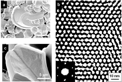
Hierarchical structure of mesoscopic silica: (a) micron sized structure - SEM image of particles with unusual curvature and thin films; (b) nanometer level structure - TEM image of monodisperse, well packed, tunable channels; (c) both micron and nanometer length scales are visible - the particle (micron) and the hexagonal internal structure (nanometer).
We have studied the mechanism under dilute acidic synthesis conditions. Upon mixing of the reagents, the system proceeds through an incubation period followed by an induction period. During the incubation period, only discrete nanometer-sized micelle structures are present. The end of the incubation period is marked by the aggregation of these micelle complexes into particles and thin films. Distinct structural ordering occurs at both the micron and nanometer length scales. [5]
Using transmission electron microscopy (TEM), we have examined the structural evolution at the nanometer length scale. The material is initially disordered, but over time, develops a hexagonally close-packed array of monodisperse channels, as shown in the following sequence. We believe this spontaneous process is the result of energy minimization by the organic amphiphilic phase.
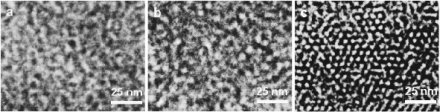
Structural evolution at the nanometer length scale. TEM images of mesoscopic silica thin film sections examined at (a) the beginning, (b) the end of the incubation period, and (c) partway through the induction period. Note the well packed channels in final image.
We have also examined the structural evolution at the micron length scale (below). Mature particles possess distinctive curvatures, while particles collected at earlier times show some evidence of amorphous structure (in the sense that the edges are not well defined).
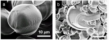
Structural evolution at the micron length scale. SEM images of particles collected after (a) 16 h and (b) 48 h of growth.
These results are useful in understanding mesoscopic silica as a self-assembling hierarchical material. The structure at both the nanometer and micron length scales occurs spontaneously due to the energy minimization interaction between the organic amphiphile and the silica gel matrix. We have found that it is possible to influence the structural ordering of mesoscopic silica at both the micron and nanometer length scales through the application of fields. [6] We are particularly interested in approaches for aligning the channels along a desired orientation, while simultaneously producing the desired micron level morphology.
In earlier work, represented by the following images, our group demonstrated that surfaces are capable of influencing the organization of the amphiphiles [7]. AFM images of adsorbed surfactant on strongly interacting surfaces such as mica (hydrophilic) and graphite (hydrophobic), reveal that the channels align in registry with the atomic lattice even though they are almost two orders of magnitude larger in diameter. On amorphous silica, the channels adopt a disordered conformation although they retain a cylindrical morphology. This is evidence that a surface field is capable of influencing the organization of the mesoscopic silica system at the early stages. The channel size is still set by self-assembly, but the choice of surface becomes a parameter by which we can control structure at higher length scales.
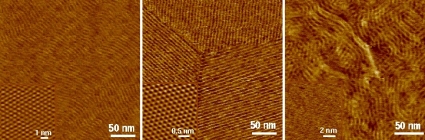
AFM images of CTAC micelles on (a) mica, (b) graphite, and (c) silica. The stripes correspond to micelle cylinders (hydrophilic mica and silica surfaces) and hemicylinders (graphite). Insets: the underlying atomic lattice of the respective substrates. [7]
We have also considered the effects of electric fields and physical confinement. [6] Micropatterned mesoscopic silica lines formed under the influence of an electric field exhibit well-ordered aligned arrays of nanometer channels, shown in the following image. Here we have attained advanced control at both the nanometer (alignment of the channels) and micron (line features) scales. We are continuing to explore the effects of applied fields (surface, confinement and electrical fields) on the structure of self-assembling hierarchical composite materials.
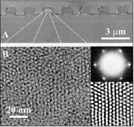
Electron microscopy of mesoscopic silica lines patterned onto a silica surface using an applied electric field and an elastomeric stamp. (a) SEM cross-section of the lines. (b) TEM image of the oriented channels. inset (top) small area electron diffraction image. (bottom) filtered image. [6]
References
![]() 1.
D.M. Dabbs, I.A. Aksay Ann. Rev. Phys. Chem. 51 601-22 (2000).
1.
D.M. Dabbs, I.A. Aksay Ann. Rev. Phys. Chem. 51 601-22 (2000).
2. N. Yao, R.Z. Wang, A.Y. Ku, D.A. Saville, I.A. Aksay, "Nanostructured Bio-inspired Materials," in Nanophase and Nanostructured Materials Z. L. Wang and Y. Liu, eds. (Tsinghua University Press and Wiley-VCH, 2001) in press.
3. C.T. Kresge, M.E. Leonowicz, W.J. Roth, J.C. Vartuli, J.S. Beck Nature 359 710-2 (1992).
4. Q.S. Huo, D.I. Margolese, G.D. Stucky Chem. Mater. 8 1147-60 (1996).
![]() 5.
N. Yao, A.Y. Ku, N. Nakagawa, T. Lee, D.A. Saville, I.A. Aksay Chem. Mat.
12 1536-48 (2000).
5.
N. Yao, A.Y. Ku, N. Nakagawa, T. Lee, D.A. Saville, I.A. Aksay Chem. Mat.
12 1536-48 (2000).
![]() 6.
M. Trau, N. Yao, Y. Xia, G.M. Whitesides, I.A. Aksay, Nature 390
674-6 (1997).
6.
M. Trau, N. Yao, Y. Xia, G.M. Whitesides, I.A. Aksay, Nature 390
674-6 (1997).
7. I.A. Aksay, M. Trau, S. Manne, I. Honma, N. Yao, L. Zhou, P. Fenter, P.M. Eisenberger, S.M. Gruner Science 273 892-8 (1996).
For more information, please contact Anthony Ku or see the Ceramic Materials Laboratory web page.
![]()
![]()
![]() © 2001 Princeton University, Ceramic Materials Laboratory.All Rights Reserved.
© 2001 Princeton University, Ceramic Materials Laboratory.All Rights Reserved.