HOME| TEXT| GRADING | STAFF | DEMOS | LECTURES | LABS| ELECTRONICS| PROGRAMS

Making Printed Circuit Boards with Orcad Layout Part 3

(Laying out the board)

bullet

Now you will create the board outline.  The things you need to consider are the following:
bullet

The size board you need.  Maybe you are mounting this into something that already exist.

bullet

Boards are priced by square inch, so don't waste space.

bullet

Yet, don't make boards too small.  It's harder for the autorouting program, and companies will charge a high density drilling fee if you have too many holes per square inch (an average of 24 holes per square inch).

bullet

Don't forget the large physical things like heat sinks, terminal blocks and mounting hardware.

bullet

Select the Obstacle button from the tool bar .

bullet

Select the Global Layer from the layer pull down list .

bullet

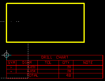
I usually place the board above the drill chart.  Click on the workspace for the lower left corner, then move up click, move right click, move down click then press ESC.  A yellow box should trace out.  Use the X Y coordinates in the upper left to determine your outline size as you trace.  Remember, I'm using mils or 1000th of an inch.  My example is 2" x 3".

 
bullet

Click on DRC so that it's gray.  The Design Rule Checker feature gets in the way at the beginning of the process.  The dotted line should disappear.

bullet

The datum is the reference place for the coordinate system.  The datum represents 0,0.  I prefer that the lower left corner of the board be 0,0.  Go to Tool -> Dimension -> Move Datum.  Click on the lower left corner to move the datum.

bullet

Select the component button from the tool bar and "TOP" for the layer .

bullet

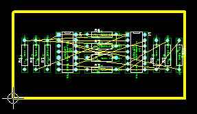
Start moving components to  within the yellow outline.

bullet

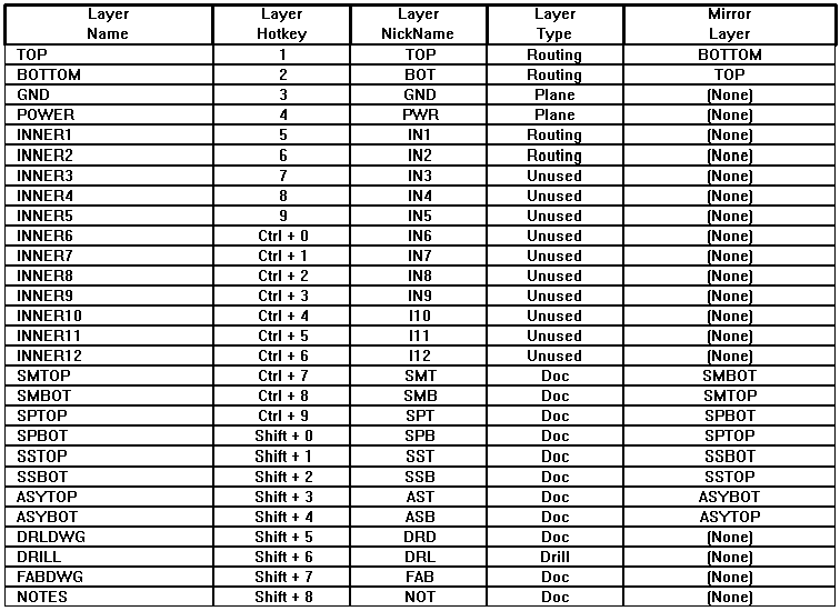
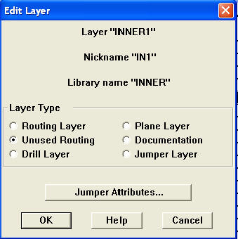
The board we are building only has a top and bottom (no inner layers), so go to Tool -> Layer -> Select from a spreadsheet ...

bullet

Select a Layer and from a right click choose "Properties" to edit the layer.  Change the GND, POWER and any INNER layer to say Unused.

bullet

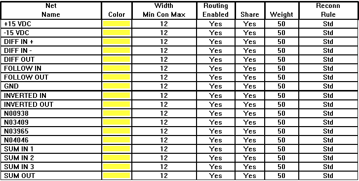
Let's take a second to look at the nets.
bullet

Go to Tool -> Net -> Select From Spreadsheet...

bullet

Press "Cancel" for the "Net Selection Criteria".

bullet

By default Capture name it's nets Nxxxxx.  Because of the ports we added in capture with good labels, we have good net names.  This will allow you to pick pins for things like headers with little confusion.  The Nxxxxx names we have are probably nets that only go from component to component and not off the board.

bullet

So from the Net names you can figure out how big of a header is needed.  I count 14 from the list, but usually I like one ground for each signal in and out so I think I need 25, (11 x 2 = 22 for signal and grounds, and 3 for power).

Go to "Making Printed Circuit Boards with Orcad Layout Part 4"

Last Modified:  10/04/04
MAE433 WEBMASTER

[ MAE224 ] [ MAE412 ]