Colored Buckles
Rebecca L. Peterson GS
Department of Electrical Engineering
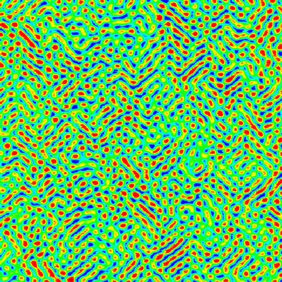
This image shows the topography of a buckled thin silicon-germanium semiconductor film measured by Atomic Force Microscopy over a 25µm x 25µm area. Under the film is a layer of glass supported by a silicon wafer. When the sample is heated to high temperature (750C), the glass flows and the film, which is initially smooth and flat but under compressive strain, forms buckles with an amplitude of about 30nm to relieve its strain. The buckles occur along the <100> crystal directions (which run roughly diagonal in this image) due to the asymmetric mechanical properties of the silicon-germanium crystal. Here, the data have been colored to highlight the periodicity and beauty of the buckles. This work was done in the lab of Professor James C. Sturm and the PRISM micro/nano fabrication facility, and is in collaboration with Karl D. Hobart of the U.S. Naval Research Lab.
|