![]()
HOME| TEXT| GRADING | STAFF | DEMOS | LECTURES | LABS| ELECTRONICS| PROGRAMS
(Getting your Capture Schematic ready for Layout)
For the purposes of demonstration, we will design a simple board in Orcad Capture and import it into Layout.
Make a schematic of a board in Orcad Capture.
Open Orcad Capture.
Select File -> New -> Design.
A blank page appears with a boarder and title block.
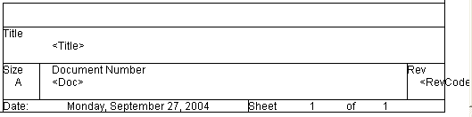
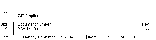
Fill out Title Block information.
See www.princeton.edu/~mae412/SCHEMATICS/titleblock.pdf for an explanation of the Title Block.
See www.princeton.edu/~mae224/labmanual/orcad_p1.doc basic Orcad Capture instruction.
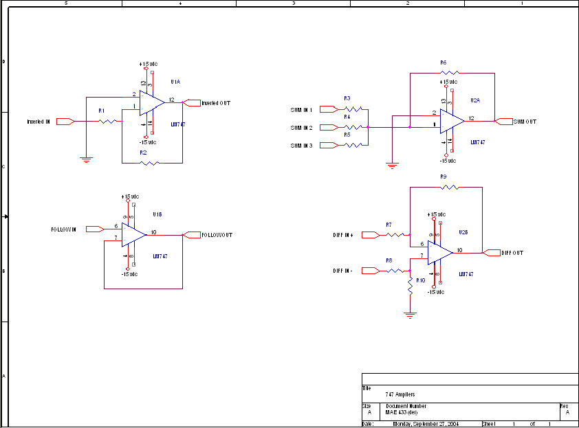
Since you are building a real board, there are things to be aware of:
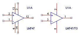
The Op Amp on the left is for a DIP chip while the right one is a metal can package (notice the different pin numbers).
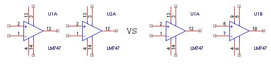
Orcad names a new chip for each part. Use unused sections of the chip to lower total number of components.
Use ports to bring signals to and off the board.
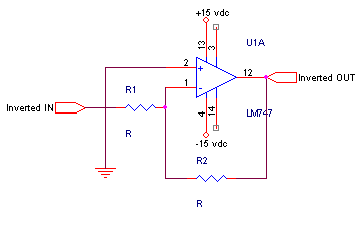
Here's the test schematic.
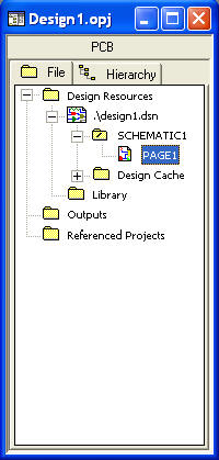
Now minimize the schematic page and select the *.opj or project window.
From the menu bar, go to Tools -> Create Netlist
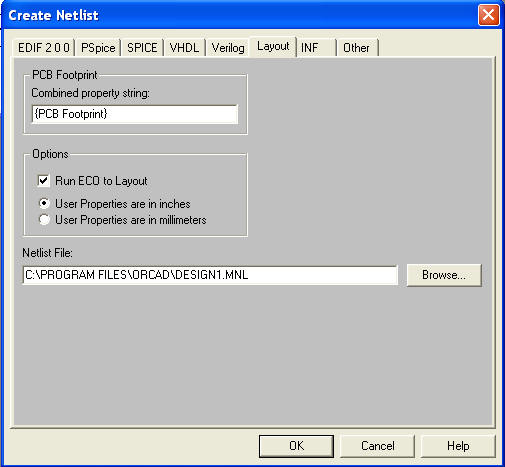
Select the Layout tab
Check off "Run ECO to Layout".
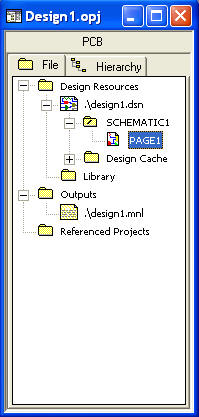
Make a note of where the *.MNL file is being created.
Notice that there is now a file listed under Outputs.
Exit out of Capture and open Layout.
Last Modified:
10/07/04
MAE433
WEBMASTER