| Dislocations
and Nanostructures
·
The electronics industry is interested in producing very small structures
that can be a part of an electronic device. Such nanostructures in silicon
may be fabricated by using the spatial properties of dislocations and their
increased chemical reactivity.
·
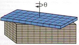
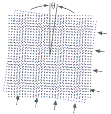
The diagrams show the regular array of screw dislocations that arise from
a pure twist boundary in a silicon crystal. This device is fabricated by
bonding a very thin crystal of silicon to a bulk substrate with a selected
missalignment, θ.
The size of the array shown in the top diagram depends upon this angle
- decreasing in linear dimension as θ
increases. |
 Click
here for an animation
Click
here for an animation