| ·
The enhanced reactivity of the dislocation regions that form the boundaries
of the domains permits them to be selectively etched leaving a series of
nanobumps on the substrate.
·
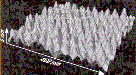
The atomic force microsope image shows the array produced by such a rotation.
The widt of the features is 25 nm corresponding to 100 silicon atoms. The
average interfeature spacing is 38 nm or 160 silicon atoms.
·
Increasing the angle of rotation decreases both the feature size and their
spacing. If the twist angle were 40, the nanobumps would be
about 5.5 nm (20 atoms) wide. For a 100 angle, the features
would be spaced at circa 2 nm. |