
Daniel Steingart, associate professor of mechanical and aerospace engineering and the Andlinger Center for Energy and the Environment
To build the world’s most cutting-edge nanotechnologies, engineers rely on lithography — a printing concept dating from the late 1700s that has evolved into an ultra-modern fabrication technology.
Now, a team of engineers from Princeton, the University of California-Los Angeles and IBM has developed a new nanolithography technique that promises greater flexibility than other methods by allowing engineers to create, analyze and erase nanoscale structures from a variety of materials.
The researchers used the technology, reported July 12 in the online journal Science Advances, to build structures less than 10 nanometers in diameter — for reference, a human hair is approximately 80,000 to 100,000 nanometers thick. The structures were so small they could only be visualized using an electron microscope.
The technique might one day be used to create anything from next-generation medical sensors and drug delivery devices to tiny lasers and better batteries.
“Fabrication of nanostructures of desired shape, structure and composition is one of the hottest areas of nanotechnology right now,” said Daniel Steingart, an associate professor of mechanical and aerospace engineering and the Andlinger Center for Energy and the Environment at Princeton. “Our new method combines several existing fabrication technologies to produce unprecedented flexibility to use in a variety of metals, build multiple types of nanostructures, and fabricate and erase those structures on the fly.”
The team based their technique on electron beam nanolithography, a technology where nanoscale structures are typically deposited in layers. The layers are laid down using an electron-sensitive film called a “resist” that changes its chemical makeup when exposed to the beam. Areas of the resist that aren’t exposed to the beam are etched away, leaving the pattern drawn by the beam intact. Every new layer requires a new resist film to be applied over the previously etched layer, so the three-dimensional nanostructure is built up stepwise as the layers stack.
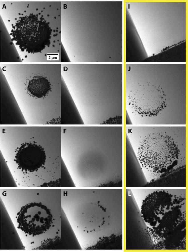
Princeton researchers including Daniel Steingart and collaborators invented a system for creating ultra-tiny structures that is more versatile than previous methods, including the ability to erase. The first two columns (images A to H) show structures that were created out of minute particles of gold then erased. Images I to L show how different structures could be created by modulating the time and electrical current of the devise. The pictures were obtained by an tunneling electron microscope, which can view objects too small to see with visible light.
This beam-centered method offers greater flexibility than techniques that used a precut mask to produce shapes, as the electron beam can draw nearly any shape. An analogy is the difference between painting words on a sign with a brush or using a precut stencil — the stencil can only produce words already cut into it, while freehand painting (electron beam lithography, in this case) can produce any word.
Current electron beam methods do, however, have some limitations. The necessity of building the layers in a stepwise fashion is slow and laborious, and the process must take place in a vacuum, which requires expensive machinery. Also, drawing on a resist film makes it difficult to fabricate alloy structures made of multiple metals.
The researchers sought to develop a method of electron beam lithography that could build nanostructures without using a resist film. To do this, they combined the beam technology with a technique for using electrical current to grow metals in a solution.
In their device, tiny metal electrodes made of gold, nickel or copper were attached to the wall of a tiny chamber filled with an electrolyte solution. To generate nanocrystals used to draw a desired shape, an electrical potential was applied across a pair of electrodes, and the electron beam was positioned between the electrodes. The electrical potential caused the electrodes to release metal ions that turned into metal when they interacted with the electrons of the beam and deposited as nanocrystals on the side of the chamber.
The device was able to print alloys as well as “core-shell” nanostructures, where one type of metal forms a shell around a core of another type. Both structures are important for various applications in nanotechnology.
In addition to creating nanostructures, the researchers used the device to erase the structures, another advance that adds to the flexibility of the device.
“We can dissolve a shape previously deposited by scanning slowly over the existing nanostructures or increasing the current to the beam already irradiating a deposit,” said Jeung Hun Park, an associate research scholar at Princeton and the IBM T. J. Watson Research Center who was lead author on the paper. “The ability to erase a structure adds another factor of control to this technique, making it a highly versatile approach to fabricating nanostructures,” Park said.
Park said the research team is now focusing on mapping the precise structure of the crystals formed by the technique, and how temperature and other parameters affect the crystalline structures. This will be important to optimizing the technology and building nanostructures with precisely defined materials.
The majority of Steingart’s research focuses on battery technology but he said the current project was not focused on immediate applications. He said the work could very well lead to better understanding of structures that improve battery performance, but in the near term the technology is more useful for experimentation and testing.
“This is more about fundamental electrochemical and electrical processing,” he said. “It is a way of saying if we had this kind of structure, how would it behave?”
Other authors on the paper were Suneel Kodambaka, of the Department of Materials Science and Engineering at the University of California-Los Angeles, and Frances M. Ross of IBM T. J. Watson Research Center.
The research was supported by the BP Carbon Mitigation Initiative and the National Science Foundation.
